Advanced Technical Ceramics, Precision Alumina, Silicon Carbide, Crucible Parts



9 Boron Nitride Applications in Semiconductor Manufacturing Engineers Should Know
1. Why Boron Nitride Matters in Semiconductor Manufacturing
In advanced boron nitride semiconductor manufacturing applications, material selection is rarely determined by a single property such as maximum temperature or dielectric strength. Semiconductor equipment engineers typically need a material to satisfy several requirements at the same time: electrical isolation at elevated temperature, dimensional stability during repeated thermal cycling, low contamination risk, compatibility with vacuum environments, sufficient thermal conductivity to prevent localized hot spots, and machinability for complex geometries. Hexagonal boron nitride, commonly abbreviated as h-BN, occupies a distinctive position among technical ceramics because it combines high electrical resistivity with useful thermal conductivity, low thermal expansion, thermal-shock resistance, chemical inertness, and relatively easy machinability. These characteristics explain why boron nitride appears in semiconductor furnaces, deposition systems, heater assemblies, vacuum components, crystal-growth equipment, evaporation systems, electrical insulation structures, and customized process hardware.
For an equipment engineer, however, the important point is that “boron nitride” does not describe one universal engineering material. Hot-pressed boron nitride, binder-free high-purity BN, binder-containing BN grades, BN ceramic composites, and pyrolytic boron nitride, or PBN, can differ significantly in purity, density, porosity, thermal conductivity, mechanical strength, dielectric behavior, moisture sensitivity, and allowable process environment. A material that performs well as a machinable high-temperature insulator may not necessarily be the correct choice for a high-purity semiconductor crucible. Similarly, a BN grade selected primarily for mechanical strength may contain a binder or secondary ceramic phase that is unacceptable in a process where trace contamination must be tightly controlled. For this reason, engineers evaluating boron nitride semiconductor manufacturing components should begin with the actual process conditions rather than selecting material from a generic BN property sheet.
The semiconductor industry places unusually strict demands on materials because a component can perform mechanically and still fail from a process perspective. A support ring may remain intact at 1,000°C but introduce unwanted impurities. An electrical insulator may provide adequate room-temperature resistance but lose reliability after repeated thermal cycling. A heater fixture may survive the peak temperature but crack because of a steep thermal gradient created during rapid ramp-up. A ceramic component may also satisfy drawing dimensions at incoming inspection yet generate particles after installation because sharp edges, incorrect mounting clearance, or excessive clamping force concentrate stress. In boron nitride semiconductor manufacturing, material qualification therefore has to consider not only nominal physical properties but also purity, microstructure, orientation, machining quality, installation method, cleaning procedure, thermal history, process gases, vacuum level, electrical field strength, and expected maintenance interval.
One reason BN is especially attractive is its combination of electrical insulation and heat transfer. Most electrical insulators are not particularly efficient heat conductors, while highly thermally conductive materials are often electrically conductive. Hexagonal boron nitride offers an unusual compromise. Momentive reports a theoretical in-plane thermal conductivity of approximately 300 W/m·K for h-BN and a volume resistivity around 10^15 Ω·cm, although the properties of a finished hot-pressed component can be substantially different because density, grain orientation, additives and processing route affect the final value. This distinction is important: an engineer should never use the single-crystal or theoretical h-BN value as the design conductivity of a machined commercial BN component without checking the exact grade and material orientation.
The layered crystal structure of h-BN is another factor engineers need to understand. Boron and nitrogen atoms are strongly bonded within individual basal planes, while the bonding between planes is much weaker. As a result, BN properties can be anisotropic. Thermal conductivity, coefficient of thermal expansion, mechanical behavior and machining response may differ with material direction. This becomes particularly important when the component is a thin plate, heater support, insulating ring, crucible wall, long tube, or part subjected to a strong one-directional temperature gradient. The engineering question is not simply whether BN has “good thermal conductivity,” but whether heat is expected to flow parallel or perpendicular to the preferred crystal orientation in the actual component. The same consideration applies when using boron nitride semiconductor manufacturing parts near concentrated heaters or rapidly changing temperature zones.
Temperature capability also requires careful interpretation. High-purity, binder-free h-BN grades can operate above 2,000°C in suitable inert or vacuum conditions, while oxidation limits in air are much lower. Saint-Gobain, for example, reports a maximum use temperature of approximately 2,000°C in inert environments for one high-purity self-bonded h-BN grade, while the listed oxidizing-atmosphere limit is approximately 850°C. This large difference illustrates why “maximum service temperature” should never be used without specifying atmosphere. Semiconductor equipment may operate in vacuum, nitrogen, argon, ammonia-containing process environments, oxygen-containing cleaning steps, or mixed reactive gases, and each condition can change the practical limit of the ceramic.
Pyrolytic boron nitride represents another important branch of the material family. PBN is produced by chemical vapor deposition rather than conventional powder pressing and sintering, giving it a very high purity and highly anisotropic layered microstructure. Shin-Etsu reports PBN purity of at least 99.999%, heat resistance around 2,400°C, and very high dielectric performance for its material, and lists applications including compound-semiconductor crucibles, MBE crucibles, semiconductor heaters and electrostatic-chuck heater structures. For contamination-sensitive boron nitride semiconductor manufacturing, this difference between PBN and conventional hot-pressed BN is fundamental. PBN may be preferred where ultra-high purity and extremely low contamination are dominant requirements, while a hot-pressed machinable BN grade may be more economical or easier to manufacture into thick, complex structural parts.
From a purchasing perspective, this means that an RFQ stating only “boron nitride part according to drawing” is incomplete for most serious semiconductor applications. The supplier needs to understand whether the component will operate in air, vacuum or process gas; its continuous and peak temperature; electrical voltage; heat flux; thermal cycling rate; acceptable metallic impurity level; whether silicon, oxygen or binder-related contamination is restricted; the required surface finish; and whether the part directly faces the wafer or process environment. These conditions determine whether the appropriate solution is conventional hot-pressed BN, a high-purity binder-free grade, a composite BN ceramic, or PBN. A robust boron nitride semiconductor manufacturing design therefore begins with process definition before dimensional manufacturing begins.
2. Key Boron Nitride Properties and Engineering Parameters for Semiconductor Equipment
When evaluating a BN component for semiconductor equipment, engineers should separate intrinsic material properties from finished-part performance. Published values are useful for preliminary screening, but they are not interchangeable across grades. A commonly cited thermal conductivity value of 300 W/m·K refers to the preferred crystal plane of h-BN; commercial hot-pressed solids can show values ranging from roughly the tens of W/m·K to well above 100 W/m·K depending on grade and direction. Saint-Gobain, for example, reports room-temperature thermal conductivity values from approximately 27–34 W/m·K for one HP grade and approximately 78–130 W/m·K for a high-purity self-bonded grade, with directional values reflecting anisotropy. This is exactly why engineers working with boron nitride semiconductor manufacturing hardware should request grade-specific data rather than copying generic internet values into a thermal model.
Table 1. Typical Engineering Parameters Relevant to Boron Nitride Semiconductor Components
| Engineering Parameter | Typical Reference Value or Range | Engineering Relevance |
|---|---|---|
| Theoretical h-BN density | Approx. 2.25 g/cm³ | Reference value; finished hot-pressed density depends on grade and porosity |
| Commercial hot-pressed BN density | Approx. 1.9–2.3 g/cm³ for many h-BN-rich grades | Influences mass, strength, porosity and thermal response |
| h-BN in-plane thermal conductivity | Up to approx. 300 W/m·K for ideal/reference material | Should not be assumed for finished machined parts |
| Typical hot-pressed BN thermal conductivity | Approx. 10–130 W/m·K depending on grade and direction | Critical for heater supports, thermal isolation and heat-spreading design |
| Volume resistivity at room temperature | Often ≥10¹³–10¹⁵ Ω·cm depending on grade | Relevant to high-voltage and heater insulation |
| Dielectric constant | Typically around 3.4–4.6 for many h-BN-rich grades | Important in RF, high-frequency and capacitive environments |
| Dielectric strength | Grade-dependent; commercial data may range from >10 to tens of kV/mm | Must be verified against thickness, geometry, temperature and test method |
| Coefficient of thermal expansion | Strongly grade- and direction-dependent; often low relative to many ceramics | Supports thermal-shock resistance but requires orientation-specific evaluation |
| Oxidizing-atmosphere temperature capability | Commonly around 850–1,000°C depending on grade | Important when equipment sees air or oxygen during operation or cleaning |
| Inert/vacuum temperature capability | Can reach approximately 2,000°C or above for suitable high-purity grades | Relevant to vacuum furnaces, deposition systems and high-temperature fixtures |
| PBN purity | High-purity commercial grades can reach ≥99.999% | Important for contamination-sensitive processes |
| PBN heat resistance | Commercial PBN data can reach approximately 2,400°C under suitable conditions | Relevant to crystal growth, evaporation and high-temperature vacuum systems |
| Machinability | High for many hot-pressed BN grades | Enables slots, threads, thin walls, holes and precision custom geometries |
| Outgassing behavior | Grade/process dependent; PBN can provide extremely low outgassing | Important in high and ultra-high vacuum environments |
The values in this table should be treated as engineering reference data rather than universal purchasing specifications. Momentive identifies h-BN theoretical density around 2.25 g/cm³, volume resistivity near 10^15 Ω·cm and dielectric constant around 4, while Saint-Gobain’s published hot-pressed BN data demonstrate how strongly density, conductivity, dielectric strength and thermal expansion can vary among commercial grades. PBN must be treated separately because its deposition-based manufacturing route produces a different structure and purity profile from powder-processed BN. This grade separation is essential in boron nitride semiconductor manufacturing, particularly when engineers are comparing material datasheets from different suppliers.
Purity should be considered as a process parameter, not simply a marketing number. A semiconductor component located outside the critical process zone may tolerate a BN composite containing a secondary phase if the composite delivers better mechanical strength or moisture resistance. A component positioned close to a wafer, evaporation source, epitaxial growth zone or high-purity melt may require much stricter control. PBN is particularly valuable in such environments because the CVD-based process can produce exceptionally high purity without conventional sintering additives. Shin-Etsu also states that its PBN machined parts contain no silicon source and are suitable where silicon contamination must be avoided. An engineer therefore needs impurity data tied to the actual grade rather than simply specifying “high-purity BN.”
Porosity is equally important. A porous BN component may still provide excellent insulation and thermal-shock resistance, but porosity can influence gas adsorption, cleaning behavior, particle generation, mechanical strength and vacuum performance. It can also affect how a component responds to wet cleaning or long exposure to ambient humidity. Binder chemistry adds another variable because some hot-pressed grades use boric oxide, calcium borate, silica or other phases to modify density, mechanical strength, moisture resistance or machining behavior. In demanding boron nitride semiconductor manufacturing systems, engineering teams should therefore review the complete composition and not only the nominal percentage of BN.
Electrical data must also be interpreted under realistic operating conditions. A dielectric-strength result measured on a polished test coupon at room temperature does not automatically predict the breakdown behavior of a thin-walled component at elevated temperature. Actual performance can be influenced by part thickness, edge geometry, electrode configuration, surface contamination, vacuum conditions, field concentration and thermal gradients. Sharp corners and narrow wall sections can increase electric-field concentration, while deposited conductive films can create leakage paths even when the original ceramic is highly insulating. Consequently, electrical design should combine material data with part geometry and expected process deposition.
Thermal modeling requires the same discipline. Because h-BN and PBN can be anisotropic, the orientation of the material relative to heat flow can change the temperature distribution across the part. PBN is an especially clear example: Shin-Etsu notes high thermal conductivity along the in-plane direction and strong thermal insulation through the thickness direction, a combination useful for uniform heating and reduced heat loss in crucible applications. In practical boron nitride semiconductor manufacturing design, orientation should therefore be defined before the component is finalized, particularly for thin plates, crucibles, heater assemblies and parts exposed to concentrated radiant heating.
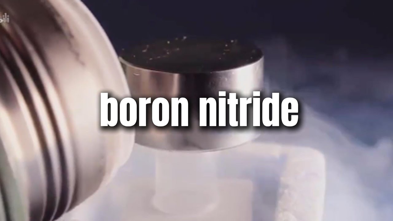
The charm of boron nitride ceramics.
3. Applications 1–3: Thermal, Electrical, and High-Temperature Components
3.1 Application 1: High-Temperature Electrical Insulators
One of the most established uses of boron nitride in semiconductor equipment is high-temperature electrical insulation. Heater assemblies, power feed structures, electrode supports, insulating spacers, sleeves, washers and fixture components may operate in environments where a polymeric insulator is impossible and where conventional ceramics can introduce limitations in machinability or thermal-shock performance. Hot-pressed h-BN is attractive because engineers can machine relatively complex geometries while retaining high electrical resistance over a broad temperature range. Saint-Gobain specifically identifies BN for electrical equipment, high-temperature furnace and semiconductor-equipment insulation, and reports dielectric performance at elevated temperatures for appropriate grades. These characteristics make electrical insulation a major category within boron nitride semiconductor manufacturing.
The design challenge is not simply to prevent a short circuit. Semiconductor heaters often combine high electrical power density, repeated ramp-up and cool-down cycles, vacuum exposure and tight spatial constraints. The insulating component may sit directly between a conductive heater element and a grounded metallic structure. If the BN part is too thin, local electric-field stress may become excessive. If it is too thick, thermal resistance may increase and alter heater uniformity. If mechanical clamping is too aggressive, thermal expansion mismatch between the ceramic and metal hardware may cause cracking. Engineers therefore need to balance dielectric path length, creepage distance, thermal conductivity, mechanical preload and expansion allowance rather than designing from dielectric-strength data alone.
Contamination further complicates the electrical design. During service, deposited material can accumulate on exposed insulating surfaces. A component that initially has extremely high surface resistance may gradually develop a conductive path due to metallic deposition, process by-products or cleaning residues. In this situation, increasing the intrinsic resistivity of the ceramic does not necessarily solve the problem. Geometric shielding, longer surface paths, removable shields and maintenance access may be more important. For boron nitride semiconductor manufacturing equipment, the best insulating component is therefore the one designed around the complete electrical and process environment rather than the BN material in isolation.
Another advantage of machinable BN is rapid development of specialized geometry. Conventional dense ceramics such as alumina or aluminum nitride frequently require diamond grinding after sintering, particularly when close tolerances or complex features are involved. Many hot-pressed BN grades can instead be machined with conventional or carbide tooling depending on composition, making prototypes and design revisions relatively practical. Saint-Gobain describes hot-pressed BN solids as machinable into complex precision components, while noting that tooling requirements change with different composite grades. For engineers qualifying a new heater assembly, this can shorten the iteration cycle between thermal simulation, prototype testing and final component design.
3.2 Application 2: Heater Supports and High-Temperature Furnace Components
Heater-support applications impose a different combination of requirements. The component may need to electrically isolate a heating element, maintain geometric positioning at temperature, survive fast temperature ramps, tolerate radiative heat flux and avoid reacting with neighboring materials. BN is particularly useful where electrical insulation and thermal-shock resistance need to coexist. In boron nitride semiconductor manufacturing, examples can include heater supports, fixture blocks, insulating plates, furnace hardware, tubes, spacers and customized structural elements used inside high-temperature vacuum or controlled-atmosphere equipment.
The engineering advantage comes from the relatively low thermal expansion of many BN grades and their resistance to rapid temperature change. Thermal shock occurs when different regions of a ceramic experience different temperatures and therefore attempt to expand by different amounts. Dense, stiff ceramics with high elastic modulus can develop large internal stresses under steep temperature gradients. BN’s layered structure, lower modulus in many grades and low expansion can provide a more forgiving thermal response. This does not make the material immune to fracture, but it can provide an important design margin when equipment repeatedly cycles between ambient and process temperature.
Material grade is particularly important here. A binder-containing grade may offer higher strength, better moisture resistance or lower cost, while a high-purity self-bonded grade may provide higher usable temperature and lower contamination risk. Published Saint-Gobain data, for example, show major differences between grades in flexural strength, thermal conductivity, porosity and maximum inert-atmosphere temperature. Therefore, an equipment engineer should not specify “BN heater support” without defining whether the priority is 1. structural strength, 2. thermal isolation, 3. heat spreading, 4. electrical insulation, 5. purity, or 6. maximum process temperature. In boron nitride semiconductor manufacturing, those priorities determine the appropriate BN formulation.
Mechanical attachment is another frequent source of failure. A ceramic heater support should generally not be treated like a ductile metallic bracket. Tight interference fits, point loading, overtightened bolts and sharp internal corners can create localized stresses that become more severe after thermal cycling. Designers should consider generous radii where possible, controlled clearances, distributed clamping, compliant interfaces and thermal-expansion differences between BN and mating metals. A component that cracks after 50 heating cycles may not indicate defective raw material; the root cause may be assembly-induced stress that was already present at room temperature.
For vacuum furnaces and deposition equipment, outgassing and material cleanliness also need to be considered. Some high-purity BN and PBN grades are particularly attractive where low outgassing is required. Shin-Etsu specifically describes PBN machined parts as higher in purity than conventional sintered BN and states that they do not produce outgassing, positioning the material for high-vacuum insulation and heater-support applications. The practical implication is that the process engineer should define vacuum requirements and contamination limits before deciding whether conventional machinable BN provides sufficient performance or whether PBN is justified.
3.3 Application 3: Thermal Management and Electrically Insulating Heat-Control Components
Thermal management is often misunderstood when discussing BN because the material is simultaneously described as thermally conductive and thermally insulating. Both statements can be valid depending on material grade, orientation, thickness and application. The engineering value of BN lies in the ability to control the path of heat while maintaining electrical isolation. In boron nitride semiconductor manufacturing, this can be useful around heater modules, power electrodes, deposition sources, temperature-control assemblies and other components where engineers need heat transfer without creating an electrical conduction path.
For hot-pressed h-BN, heat conduction is strongly influenced by grain orientation created during pressing. A component can therefore display different conductivity along different axes. This anisotropy should be incorporated into finite-element thermal simulations whenever temperature uniformity is critical. Using a single isotropic conductivity number can underestimate or overestimate local temperatures, particularly in thin plates or long components. PBN has even stronger directional behavior, and this property is deliberately used in some crucible and heater-related applications. Shin-Etsu describes PBN as having high in-plane thermal conductivity while providing thermal insulation through its thickness, which can help distribute heat along a surface while limiting heat transfer in the perpendicular direction.
This directional behavior can be valuable around semiconductor heating systems where temperature uniformity directly affects process stability. A localized hot spot can change deposition rate, induce thermal stress in neighboring components, shift wafer temperature uniformity or accelerate degradation of seals and electrical hardware. A properly oriented BN component can help spread heat or isolate it depending on the design objective. However, engineers should avoid assuming that simply replacing alumina or another ceramic with BN will automatically improve thermal performance. The design should compare actual grade conductivity, orientation, component thickness, contact resistance and operating temperature.
Contact resistance is often as important as bulk conductivity. A BN plate may have relatively high thermal conductivity, but if surface flatness is poor or the mechanical preload is insufficient, microscopic gaps at the interface can dominate the thermal path. Conversely, excessive preload can damage a relatively soft machinable BN component. Surface finish, flatness, mating-material condition and clamping strategy must therefore be included in the thermal design. For this reason, boron nitride semiconductor manufacturing components intended for heat-transfer functions should be specified with mechanical interface requirements in addition to bulk material properties.
Engineers should also distinguish between using BN as a heat-spreading solid component and using BN powder as a thermally conductive filler. BN-filled polymers, thermal interface materials and electronic encapsulants represent a different application class from structural semiconductor-equipment components. The same underlying combination of electrical insulation and thermal conductivity is useful, but the design rules, contamination requirements and service temperatures are completely different. For semiconductor process equipment, the relevant decision usually concerns a machined hot-pressed BN part, high-purity BN component or PBN structure rather than a polymer composite.
The practical engineering conclusion from these first three applications is that BN performs best when its electrical, thermal and manufacturing characteristics are considered together. A heater insulator, furnace support or thermal-control component cannot be specified correctly from one material property. The engineer must define 1. process temperature, 2. atmosphere or vacuum level, 3. electrical voltage, 4. heat-flow direction, 5. thermal ramp rate, 6. purity requirement, 7. acceptable secondary phases, 8. mechanical loading, 9. mounting method and 10. dimensional tolerances. When these conditions are defined correctly, boron nitride semiconductor manufacturing components can be engineered as functional process hardware rather than treated as generic ceramic replacements.
4. Applications 4–6: Vacuum, Deposition, and Plasma Processing Equipment
4.1 Application 4: Boron Nitride Components in CVD and MOCVD Equipment
Chemical vapor deposition and metal-organic chemical vapor deposition systems impose one of the most demanding combinations of temperature, chemical exposure, electrical isolation and contamination control found in semiconductor production equipment. In these systems, engineers are rarely selecting a ceramic simply because it can tolerate a high nominal temperature. The actual component may be located near a heated susceptor, process-gas delivery path, heater assembly, substrate carrier or deposition source, and it may experience simultaneous thermal gradients, reactive gases, vacuum conditions and repeated process cycling. For this reason, boron nitride semiconductor manufacturing applications in CVD and MOCVD equipment should be evaluated from a complete process-environment perspective rather than from a single datasheet value.
One important application is the use of PBN around graphite-based heating and process components. Graphite is widely used where high-temperature capability and electrical conductivity are required, but its exposed surface may react with certain process atmospheres or become a potential contamination source. PBN coatings can provide a chemically stable, electrically insulating and high-purity barrier between the graphite substrate and the process environment. Shin-Etsu specifically identifies PBN-coated graphite heaters, susceptors and reflectors for high-temperature processes and notes that PBN coating can help protect graphite in NH₃-containing MOCVD conditions. In its published NH₃ resistance testing, the coated material maintained resistance up to 1,400°C without measurable weight change under the stated test conditions. This is highly relevant to boron nitride semiconductor manufacturing because ammonia exposure is a major materials consideration in III-nitride MOCVD equipment.
The engineering significance of a PBN coating extends beyond corrosion resistance. A coating can electrically isolate a conductive graphite body, alter radiant-heat behavior and reduce direct interaction between the process environment and the underlying carbon material. However, a PBN coating should not be treated as a generic paint layer. Deposition thickness, substrate thermal-expansion behavior, surface preparation, geometry and local stress all influence coating reliability. Shin-Etsu reports typical PBN coating thicknesses of approximately 20–400 μm for its coated graphite products and specifically notes that deep narrow gaps are difficult to coat uniformly. Therefore, a design that works well as a machined graphite component may require geometric modification before it becomes a reliable PBN-coated component.
A common engineering mistake is to specify a PBN coating after the mechanical design is already complete. From an equipment-design perspective, coating feasibility should be reviewed at the same time as geometry. Long blind holes, deep recesses, sharp internal corners and extreme thickness transitions can create nonuniform deposition conditions or localized stress. For boron nitride semiconductor manufacturing, the coating specification should therefore include 1. graphite substrate grade, 2. required coating thickness, 3. exposed process surfaces, 4. maximum operating temperature, 5. process atmosphere, 6. acceptable coating defects, 7. dimensional tolerance after coating and 8. whether a high-emissivity surface is required.
PBN is also used as a structural or machined component in MOCVD-related systems. Shin-Etsu lists high-temperature gas pipes for MOCVD equipment among its PBN machined-part applications. This demonstrates an important distinction between a PBN coating and a freestanding PBN component. A coating relies on the mechanical support of the graphite substrate, whereas a PBN machined component relies on the deposited PBN body itself. The correct choice depends on geometry, thickness, mechanical loading and required thermal behavior. Where a thick structural section is needed, PBN-coated graphite may be more practical than a thick freestanding PBN component; where ultra-high purity and electrical insulation dominate, a freestanding PBN part may provide greater process isolation.
Thermal behavior is especially important near CVD heaters. PBN is strongly anisotropic, meaning heat conduction differs dramatically with material direction. Shin-Etsu reports thermal conductivity values for its PBN of approximately 50–60 W/m·K in the in-plane direction for its standard density grade and approximately 1.8 W/m·K through thickness, while a higher-density version reaches approximately 110 W/m·K in-plane. For boron nitride semiconductor manufacturing, this means PBN can simultaneously spread heat along one direction and restrict heat transfer through another. Properly oriented, this can be useful for improving heater uniformity or reducing unwanted heat loss. Improperly oriented, the same anisotropy can produce a thermal field very different from what an isotropic simulation predicts.
PG/PBN heater technology further demonstrates how these properties can be integrated into semiconductor equipment. Shin-Etsu publishes PG/PBN heater applications for sputtering and CVD systems and reports demonstrated vacuum operation up to 1,600°C, heating rates up to 810°C/s for a heater unit, temperature uniformity of 900°C ±2.5°C over an 8-inch wafer in a stated test configuration, and more than 10,000 thermal cycles between 200°C and 1,200°C. These are supplier-specific demonstrated values rather than universal PBN specifications, but they illustrate why thin PBN/pyrolytic-graphite structures are attractive when rapid thermal response, electrical isolation and high-vacuum compatibility are required.
For engineers, the larger lesson is that CVD and MOCVD components should be specified according to function rather than material name. A heater insulator, gas pipe, susceptor coating and radiant shield may all contain BN, yet their design criteria are different. In boron nitride semiconductor manufacturing, the correct engineering question is therefore not “Can BN survive this temperature?” but rather “What BN form, orientation, purity and geometry will remain stable under this specific combination of temperature, gas chemistry, voltage, heat flux and thermal cycling?”
4.2 Application 5: PVD, Sputtering, and High-Vacuum Equipment Components
Physical vapor deposition systems create a different set of engineering constraints. Vacuum quality, electrical fields, radiant heating, conductive deposition and particle control become particularly important. A component near a sputtering source or evaporation source may begin as an excellent electrical insulator but gradually become coated with conductive material during process operation. Consequently, material selection and component geometry must account for both initial performance and the condition of the component after hundreds or thousands of process cycles. This is an important consideration in boron nitride semiconductor manufacturing, where equipment reliability depends not only on initial ceramic properties but also on how those properties evolve in the process chamber.
PBN and high-purity BN are attractive in high-vacuum systems because they combine electrical insulation with high-temperature capability and low contamination potential. Shin-Etsu lists high-vacuum insulation components and heater supports among PBN machined-part applications and describes its PBN sheet products as providing electrical insulation under high-temperature and ultra-high-temperature vacuum conditions. PBN is produced by chemical vapor deposition rather than conventional powder sintering, and the resulting dense layered structure eliminates the conventional sintering additives that may be undesirable in highly contamination-sensitive processes.
Outgassing is one of the most important selection criteria in vacuum equipment. Materials that absorb moisture or contain volatile secondary phases can increase pump-down time, destabilize base pressure or introduce contaminants into a process chamber. Shin-Etsu describes its PG/PBN heater as suitable for high-vacuum processes and attributes its low outgassing behavior partly to the dense CVD structure without the grain boundaries typical of sintered materials. In boron nitride semiconductor manufacturing, this distinction can justify the use of PBN instead of conventional hot-pressed BN for components positioned directly in a critical vacuum process zone.
However, low outgassing should never be assumed from the word “BN” alone. Hot-pressed boron nitride grades can contain binders or secondary phases, and their open porosity may differ substantially. A machinable BN composite that performs extremely well as an atmospheric heater insulator may not be the optimum choice for an ultra-high-vacuum deposition chamber. Engineers should therefore request 1. exact composition, 2. density, 3. porosity information, 4. binder chemistry, 5. cleaning recommendations, 6. bake-out capability and 7. vacuum-use history before approving a grade for critical service.
Sputtering systems also require careful thermal design. A ceramic component may sit near a heated substrate, target assembly, bias electrode or high-current power structure. In those positions, electrical insulation and heat transfer cannot be considered separately. Shin-Etsu’s PBN/PG heater products are specifically identified for sputtering and CVD equipment, while its PBN electrostatic-chuck technology is intended for high-temperature sputtering and ion-implantation applications. These examples show how PBN can serve as both an electrical barrier and a thermal-management material in boron nitride semiconductor manufacturing equipment.
Conductive coating accumulation must also be considered. In a sputtering chamber, deposited metal may progressively cover an insulating surface. Once the coating bridges between conductive regions, the system can develop leakage current, arcing or unstable bias behavior even though the underlying ceramic remains electrically intact. Good component design can reduce this risk through 1. shadowed insulation surfaces, 2. extended creepage paths, 3. replaceable shielding, 4. controlled edge geometry and 5. maintenance-friendly installation. These design decisions are often more important than simply specifying a higher room-temperature dielectric strength.
Particle generation represents another major concern. Machined BN is relatively soft compared with dense alumina or silicon carbide, which can be advantageous for machining but requires thoughtful mechanical design. Unprotected edges can chip during installation, and excessive bolt preload can damage thin sections. In boron nitride semiconductor manufacturing, engineers should avoid locating fragile edges directly in high-contact maintenance zones and should specify edge breaks, radii, mounting clearances and handling procedures on the drawing. A ceramic component that is technically suitable for the process can still become a yield risk if its mechanical installation encourages repeated edge damage.
4.3 Application 6: Plasma Processing and Electrical Isolation Components
Plasma processing introduces additional complexity because chemical compatibility may become more important than high-temperature capability. Etch, clean and deposition plasmas can contain fluorine-, chlorine-, oxygen- or hydrogen-based reactive species, and a ceramic that is stable in vacuum may not be stable under direct plasma exposure. For this reason, boron nitride semiconductor manufacturing components used around plasma equipment require a location-specific assessment. A BN part positioned behind a shield or outside the active plasma region may perform very differently from the same material directly exposed to energetic ions and reactive radicals.
This is an area where engineers should avoid broad claims that boron nitride is “plasma resistant.” Compatibility depends on the exact plasma chemistry, ion energy, temperature and material grade. One useful real-world limitation comes from Shin-Etsu’s PBN electrostatic-chuck information, which states that its specific PBN ESC cannot be used in a fluorine plasma atmosphere. That supplier-specific limitation should not be generalized to every BN component, but it illustrates the correct engineering mindset: plasma compatibility must be validated for the actual process, not inferred from high-temperature stability or chemical inertness under non-plasma conditions.
Electrical isolation remains a major reason to consider BN near plasma-generation and substrate-bias systems. Components may need to isolate a powered electrode, heater or sensor from grounded structures while simultaneously tolerating elevated temperature. High resistivity and relatively low dielectric loss can be useful in these environments, but electric-field concentration must be controlled. Thin edges, drilled holes, sharp corners and contamination films can dramatically change local field strength. In boron nitride semiconductor manufacturing, a reliable insulator therefore requires coordination among the material engineer, electrical engineer and mechanical designer.
Temperature can further alter the electrical design. Room-temperature volume resistivity is useful for material screening but cannot alone define high-temperature insulation performance. Process temperature, surface deposition, vacuum level and electrode configuration all influence leakage behavior. Engineers should request temperature-dependent electrical property data where the application is critical and should not assume that a room-temperature dielectric-strength value remains constant at 500°C, 800°C or higher.
In plasma-adjacent applications, cleaning strategy must also be addressed at the design stage. If the BN component must be periodically cleaned, the cleaning chemistry, ultrasonic exposure, mechanical wiping and bake-out procedure should be qualified. A cleaning method that removes deposition effectively may roughen the surface or damage thin edges. In boron nitride semiconductor manufacturing, maintenance compatibility can be as important as first-cycle process compatibility because many semiconductor tools are expected to operate through repeated preventive-maintenance intervals.
The engineering conclusion for Applications 4–6 is therefore highly process-specific. CVD and MOCVD applications emphasize gas chemistry, thermal cycling, purity and coatings; PVD and high-vacuum systems emphasize outgassing, electrical isolation, deposition buildup and particle control; plasma systems add reactive-species compatibility and surface erosion. BN can solve difficult combinations of these requirements, but the correct material family and geometry must be selected after the actual process environment is defined.
5. Applications 7–9: Crystal Growth, Crucibles, MBE, and Precision Semiconductor Components
5.1 Application 7: PBN Crucibles for Compound Semiconductor Crystal Growth
PBN crucibles are among the most technically significant examples of boron nitride in semiconductor materials processing. Compound-semiconductor crystal growth requires extremely careful control of contamination because the crucible is in direct contact with high-purity source material at elevated temperature for extended periods. In this environment, mechanical strength alone is not sufficient. The crucible material must combine chemical stability, high purity, controlled thermal behavior and resistance to thermal cycling. For this reason, boron nitride semiconductor manufacturing frequently uses PBN in applications involving GaAs, InP and other compound semiconductor materials.
Shin-Etsu identifies PBN crucibles for III-V compound semiconductor growth, including GaAs and InP, and provides designs for Liquid Encapsulated Czochralski, Vertical Gradient Freezing, Vertical Bridgman and Horizontal Bridgman processes. Each growth method creates a different thermal and mechanical condition. LEC systems require geometry compatible with the melt and encapsulation arrangement. VGF and VB systems depend strongly on controlled axial temperature gradients, while horizontal Bridgman systems use elongated boat geometries. Consequently, crucible selection should begin with the crystal-growth method rather than with a generic PBN vessel specification.
Purity is the first major reason for using PBN. Shin-Etsu reports representative metallic impurity concentrations generally below the ppm level for multiple elements in its PBN material, while its broader PBN data describe the material as an ultra-high-purity ceramic produced by CVD from BCl₃ and NH₃. In boron nitride semiconductor manufacturing, this CVD route is important because it avoids many of the sintering additives that may be present in conventional hot-pressed ceramics. Where the crucible directly contacts semiconductor source material, even trace impurities can become relevant to electrical properties, defect formation or subsequent device performance.
Thermal anisotropy is the second important factor. PBN conducts heat much more effectively along its deposited layers than through its thickness. This behavior can help distribute heat circumferentially while limiting heat loss through the crucible wall. Shin-Etsu describes this combination as useful for achieving uniform heating while minimizing thermal energy loss. From an engineering standpoint, this means wall orientation and deposition structure are part of the crucible design, not merely material-science details.
Geometry also influences crystal-growth stability. Wall thickness, bottom radius, taper, straightness and surface condition can influence temperature distribution and melt behavior. In boron nitride semiconductor manufacturing, a crucible should therefore be treated as a functional thermal component rather than a passive container. A dimensional deviation that would be insignificant in ordinary ceramic ware may change heat transfer or material loading in a precision growth process.
Surface finish can become particularly important when the crucible is used repeatedly or when residue removal is required between runs. Shin-Etsu offers inner-surface polishing and cleaning treatments for PBN crucibles used in MBE-related applications, demonstrating that surface condition is a recognized process variable. Engineers evaluating suppliers should therefore consider not only nominal purity but also as-manufactured surface quality, cleaning method, packaging and handling controls.
Lifetime cannot be assigned from material name alone. The same crucible may experience very different life depending on maximum temperature, thermal ramp rate, melt chemistry, cleaning method and mechanical handling. Shin-Etsu explicitly notes that PBN crucible reuse depends on the actual operating environment rather than a fixed universal lifetime. This is a useful purchasing principle for boron nitride semiconductor manufacturing: engineers should compare suppliers on process history, dimensional control and material consistency rather than asking only for a guaranteed number of cycles.
5.2 Application 8: MBE and Electron-Beam Evaporation Components
Molecular beam epitaxy imposes some of the highest purity requirements in semiconductor thin-film processing. Source materials are heated in vacuum and directed toward the substrate under tightly controlled conditions. The crucible or source container must therefore contribute minimal contamination while maintaining dimensional and thermal stability at process temperature. PBN is widely used for this reason, and Shin-Etsu specifically identifies PBN source crucibles for MBE deposition on semiconductor wafers. This makes MBE one of the most technically demanding examples of boron nitride semiconductor manufacturing.
In an MBE source, temperature uniformity influences evaporation behavior and therefore flux stability. Because PBN is highly anisotropic, its heat-flow characteristics can be used to control temperature distribution in the source container. However, engineers must evaluate the entire heater-crucible assembly. The heater radiation pattern, crucible wall thickness, coating, source fill level and thermal contact all influence the actual temperature profile.
Some PBN crucibles use additional surface coatings to adjust heat absorption. Shin-Etsu offers pyrolytic-graphite coating and a proprietary insulating coating for certain MBE crucibles, with published coating thicknesses of approximately 20–100 μm. The reason is straightforward from an engineering perspective: changing surface emissivity changes radiant heat absorption, which can influence crucible temperature and heater efficiency. Therefore, in boron nitride semiconductor manufacturing, coating selection can be part of thermal design rather than simply corrosion protection.
Electron-beam evaporation presents a different challenge. The electron beam concentrates substantial energy into a relatively small region, producing steep thermal gradients. Shin-Etsu identifies PBN hearth liners for electron-beam evaporation and states that the material’s anisotropic layered structure helps distribute thermal stress between layers. It also applies conductive pyrolytic-graphite coatings in some designs to dissipate charge generated by the electron beam. This is an excellent example of how electrical and thermal requirements interact in semiconductor process hardware.
Charge accumulation should not be overlooked. PBN is highly electrically insulating, which is valuable in many applications but can create difficulties where electron bombardment produces surface charge. In EB evaporation, a conductive coating can provide a controlled charge-dissipation path while retaining the thermal and chemical advantages of the PBN structure. In boron nitride semiconductor manufacturing, the engineer should therefore avoid treating electrical insulation as an unconditional advantage. The correct electrical behavior depends on whether the component needs to block current, dissipate charge or perform both functions in different regions.
Source-material compatibility should also be reviewed individually. PBN has broad chemical stability, but no crucible material should be described as universally inert to every evaporant at every temperature. Engineers should evaluate the intended source material, maximum temperature, vapor pressure, wetting behavior and potential reaction products. Where contamination risk is extremely high, actual application history with the specific source chemistry can be more valuable than a generic corrosion-resistance statement.
5.3 Application 9: Custom Precision Boron Nitride Parts for Semiconductor Equipment
The ninth application category is broader but commercially important: custom machined BN and PBN components used throughout semiconductor equipment. These parts may include insulating rings, heater supports, spacers, plates, tubes, gas-handling components, fixtures, masks, evaporation hardware and customized high-temperature structures. The value of BN in this category comes from the ability to combine thermal performance, electrical insulation and relatively flexible component geometry. For many boron nitride semiconductor manufacturing projects, the engineering challenge is not whether BN can perform the required function, but which BN grade can be manufactured reliably into the required shape.
Hot-pressed BN is particularly attractive for complex machined parts because many grades can be machined more readily than dense structural ceramics such as alumina or silicon nitride. This can reduce prototype lead complexity and allow threads, grooves, slots, thin sections and nonstandard holes to be produced without the extensive diamond grinding often required for harder ceramics. However, machinability does not mean the material should be designed like aluminum or stainless steel. BN remains a ceramic, and sharp internal corners, extremely thin unsupported walls and excessive mechanical preload can create failure risks.
PBN provides a different manufacturing envelope. Because it is deposited by CVD, PBN is well suited to thin shells, crucibles, sheets and certain complex deposited structures, but it is not always the economical choice for thick structural blocks. Shin-Etsu notes that for some applications requiring PBN sections thicker than approximately 5 mm, PBN-coated graphite may be recommended instead of a fully PBN structural part. For boron nitride semiconductor manufacturing, this illustrates why grade selection and manufacturing-process selection are inseparable.
A precision drawing should therefore communicate functional requirements in addition to dimensions. The engineer should specify 1. critical surfaces, 2. datum structure, 3. flatness, 4. parallelism, 5. perpendicularity, 6. hole tolerance, 7. edge condition, 8. surface finish and 9. whether particular surfaces directly face the wafer or plasma environment. Applying the same tight tolerance to every dimension increases cost without necessarily improving equipment performance.
Cleaning and packaging should also be included in the component specification. A dimensionally perfect BN part can still become unsuitable for semiconductor service if it is contaminated during machining, handling or packaging. In boron nitride semiconductor manufacturing, final inspection should therefore address not only geometric conformity but also visible contamination, machining debris, edge integrity and packaging cleanliness appropriate to the intended process.
Supplier communication becomes especially important for first-time designs. Engineering drawings often show the desired final geometry but not the reason for each feature. If the ceramic supplier understands which surfaces are electrical barriers, which faces transfer heat, which regions enter the vacuum chamber and which dimensions control assembly alignment, manufacturing recommendations can be much more useful. This collaborative design approach can reduce unnecessary tolerance, lower fracture risk and improve reproducibility between prototype and production batches.
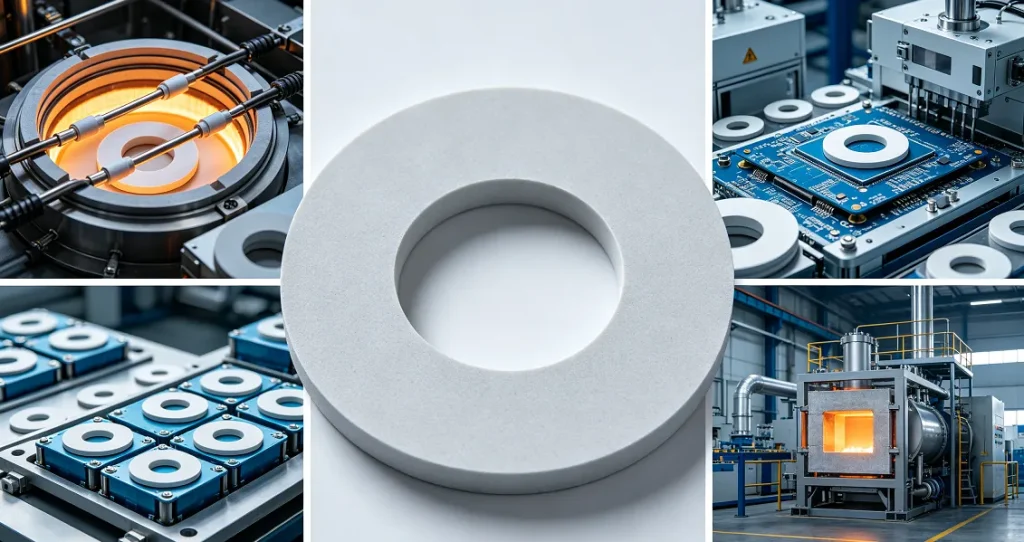
6. How Engineers Should Select Boron Nitride Grades for Semiconductor Manufacturing
Selecting the correct BN grade requires a structured engineering process. A purchasing specification that says only “99% boron nitride” is rarely sufficient because two materials with similar nominal BN content may have different binder chemistry, density, porosity, thermal conductivity, mechanical strength and vacuum behavior. Likewise, selecting PBN solely because it has the highest purity may increase cost without improving equipment performance where contamination is not the controlling requirement. For boron nitride semiconductor manufacturing, the most reliable approach is to define the operating condition first and then identify the material family that best matches it.
Table 2. Engineering Selection Guide for Boron Nitride Semiconductor Components
| Process or Design Condition | Primary Engineering Concern | BN Material Starting Point | Why It May Be Suitable | What the Engineer Must Confirm |
|---|---|---|---|---|
| High-temperature electrical insulation | Resistivity, dielectric strength, thermal cycling | Hot-pressed high-purity BN | Machinable, electrically insulating, thermal-shock resistant | Voltage, temperature, wall thickness, creepage distance |
| High-vacuum heater support | Outgassing, purity, electrical insulation | High-purity BN or PBN | Low contamination potential and high-temperature insulation | Vacuum level, bake-out, binder content, porosity |
| MOCVD graphite heater or susceptor | NH₃ exposure, graphite protection | PBN-coated graphite | Combines graphite structure with protective PBN surface | Coating thickness, substrate grade, geometry, thermal expansion |
| CVD or sputtering heater | Temperature uniformity and rapid response | PG/PBN heater structure | Thin structure, anisotropic heat transfer, high-vacuum compatibility | Power density, heating rate, wafer size, zone design |
| GaAs or InP crystal growth | Ultra-high purity and melt compatibility | PBN crucible | High purity, thermal anisotropy, chemical stability | Growth method, geometry, surface finish, cleaning method |
| MBE source crucible | Purity, flux stability, thermal distribution | PBN | Suitable for high-purity source containment and controlled heating | Source material, heater configuration, coating, crucible dimensions |
| EB evaporation | Thermal shock and charge management | PBN or coated PBN design | Layered structure can manage thermal gradients | Beam power, charge dissipation, source chemistry |
| Complex thick machined component | Geometry, machinability, cost | Hot-pressed BN or BN composite | Easier machining of complex structural shapes | Binder chemistry, purity, minimum wall thickness |
| Thick PBN-function component | Purity plus structural thickness | PBN-coated graphite may be considered | Provides PBN process surface with graphite mechanical support | Coating adhesion, exposed graphite risk, thermal expansion |
| Plasma-adjacent insulation | Electrical isolation and plasma compatibility | Grade-specific BN evaluation | Can provide insulation outside aggressive plasma zones | Exact plasma chemistry, ion energy, erosion rate |
| Wafer-facing high-purity component | Particle and metallic contamination | High-purity BN or PBN | Reduced impurity contribution | Trace-element limits, surface condition, cleaning and packaging |
The table should be used as a material-screening framework rather than an automatic grade-selection chart. Final selection depends on the actual process and supplier-specific material data. For example, Shin-Etsu reports PBN densities of approximately 1.99 g/cm³ and 2.15 g/cm³ for two density variants, in-plane thermal conductivity of approximately 50–60 W/m·K and 110 W/m·K respectively, volume resistivity above 10^14 Ω·cm and a stated maximum inert-environment service temperature of 2,400°C. Those values demonstrate the performance envelope of specific PBN materials but should not be automatically assigned to every PBN product in boron nitride semiconductor manufacturing.
6.1 Selection Factor 1: Start With Process Atmosphere
The first selection variable should be atmosphere. An engineer should define whether the component operates in 1. air, 2. inert gas, 3. high vacuum, 4. ultra-high vacuum, 5. ammonia, 6. hydrogen-containing gas, 7. oxygen-containing gas or 8. direct plasma exposure. Atmosphere can completely change the practical temperature limit of a BN component. A grade capable of extreme temperature in inert conditions may have a much lower usable temperature in an oxidizing atmosphere.
For boron nitride semiconductor manufacturing, this is especially important because equipment can experience more than one atmosphere during its life cycle. A component may operate under vacuum during deposition but be exposed to air during venting, oxygen during chamber cleaning and humid ambient conditions during maintenance. Material qualification should therefore consider not only the production recipe but also startup, shutdown, chamber clean and preventive maintenance.
6.2 Selection Factor 2: Define Purity Based on Component Location
Purity should be tied to contamination risk. A BN part inside an external heater cabinet does not necessarily require the same impurity limits as a crucible directly contacting compound-semiconductor source material. Engineers should classify the component by proximity to the critical process zone and by the probability that impurities can reach the wafer or source material.
In boron nitride semiconductor manufacturing, a useful hierarchy is 1. non-process structural region, 2. vacuum-chamber region, 3. process-facing region and 4. direct source-material contact. As the component moves closer to direct process contact, requirements for metallic impurities, binder chemistry, silicon content, cleaning and packaging generally become more important. PBN is particularly attractive at the high-purity end because it is produced through CVD and can achieve very low metallic impurity levels.
6.3 Selection Factor 3: Separate Thermal Conductivity From Thermal Control
High thermal conductivity is not always the goal. Some components need to spread heat, while others need to block it. BN is valuable because different grades and orientations can support both functions. PBN provides a particularly strong example because its in-plane conductivity can greatly exceed its through-thickness conductivity.
An engineer designing boron nitride semiconductor manufacturing equipment should therefore define the desired heat-flow direction before selecting material. For a heater plate, lateral heat spreading may improve temperature uniformity. For an insulating spacer, low through-thickness conductivity may reduce heat leakage. For a crucible, anisotropic conductivity may influence source-material temperature uniformity. The required property is not simply “high k” or “low k,” but controlled heat flow.
6.4 Selection Factor 4: Review Electrical Performance at Operating Temperature
Electrical insulation must be evaluated at the actual process temperature and geometry. Published room-temperature resistivity and dielectric strength are useful screening tools, but final design must account for temperature, thickness, surface contamination, vacuum conditions and field concentration.
In boron nitride semiconductor manufacturing, engineers should identify 1. maximum voltage, 2. DC or RF operation, 3. expected leakage limit, 4. minimum insulation thickness, 5. creepage distance and 6. potential deposition paths. A thick high-resistivity ceramic can still fail electrically if conductive deposition bridges its surface or if a sharp metal edge concentrates the field.
6.5 Selection Factor 5: Match Mechanical Design to Ceramic Behavior
BN is machinable, but machinability should not be confused with ductility. The component remains a ceramic and should be protected from tensile stress, impact and point loading. Thin unsupported walls, sharp internal corners and excessive bolt torq
7. Common Failure Modes of Boron Nitride Components in Semiconductor Equipment
Boron nitride components are often selected because they combine electrical insulation, thermal stability, machinability, low thermal expansion, and compatibility with high-temperature or vacuum environments. However, these advantages do not eliminate the possibility of premature component failure. In practical boron nitride semiconductor manufacturing, most failures are not caused by a single material property. They usually result from an interaction among material grade, geometry, mounting method, process temperature, thermal gradients, contamination, cleaning procedures, and mechanical handling. For engineers, understanding how BN components fail is therefore just as important as understanding why they are selected.
A cracked BN support, chipped heater insulator, contaminated crucible, or warped precision component should not automatically be classified as a raw-material defect. In many cases, the failure mechanism can be traced to inappropriate grade selection, excessive assembly stress, improper thermal cycling, unsuitable cleaning, or incorrect dimensional tolerancing. A systematic failure analysis should consider the entire service history of the component, including incoming inspection, installation, process startup, normal production, preventive maintenance, chamber cleaning, and removal.
7.1 Failure Mode 1: Thermal Cracking From Excessive Temperature Gradients
Thermal cracking is one of the most common failure mechanisms in ceramic components used near heaters, furnaces, evaporation sources, and deposition systems. Even though boron nitride generally has good thermal-shock resistance, a sufficiently large temperature difference across a component can still generate stresses that exceed the local strength of the ceramic. This can occur when one surface is exposed directly to a heater while another surface is mechanically constrained or cooled by a metallic mounting structure.
In boron nitride semiconductor manufacturing, the risk becomes greater when the component contains abrupt changes in cross section. A thick section connected directly to a thin wall does not heat and cool at the same rate. The thin section responds rapidly, while the thicker region may remain cooler for longer. This temperature difference produces differential expansion and can create tensile stress at the transition zone. Sharp corners make the situation worse because stress becomes concentrated in a smaller area.
An engineer investigating repeated cracking should therefore examine not only the maximum process temperature but also the heating rate, cooling rate, local heat flux, temperature uniformity, and actual contact conditions. A BN component rated for a high temperature can still fail at a substantially lower temperature if the thermal gradient is sufficiently severe.
Finite-element thermal analysis is useful when the part operates close to a heater or undergoes rapid cycling. The analysis should use grade-specific thermal conductivity and thermal-expansion data rather than generic BN values. Because many BN materials are anisotropic, the conductivity direction should also be included in the model. Ignoring anisotropy may underestimate the temperature difference across a component and therefore underestimate thermal stress.
For critical boron nitride semiconductor manufacturing equipment, engineers should also examine whether the heating profile can be modified. Slower ramp rates, improved heater uniformity, reduced contact with cold metallic structures, or changes in part thickness can sometimes solve a cracking problem without changing material grade.
7.2 Failure Mode 2: Edge Chipping and Mechanical Fracture
Hot-pressed boron nitride is relatively easy to machine compared with many dense engineering ceramics, but this does not mean it behaves like a metal. BN components remain brittle and can be damaged by impact, excessive clamping force, poor handling, or concentrated contact loads. Thin edges, sharp corners, narrow slots, and small threaded regions are particularly vulnerable.
In boron nitride semiconductor manufacturing, edge chipping can create two problems simultaneously. The first is structural damage. The second is particle contamination. Even a small chip that does not compromise the mechanical function of the component may be unacceptable if loose ceramic particles can enter a wafer-processing region, deposition chamber, or precision vacuum system.
For this reason, drawings should normally avoid unnecessarily sharp external edges. A controlled edge break or small radius can substantially reduce handling damage. Internal corners should also use practical radii wherever the design allows. A perfectly sharp internal corner may appear desirable in CAD, but it can create both machining difficulty and a strong local stress concentration.
Clamping design requires similar attention. A bolt tightened directly onto a BN surface can create high local compressive stress under the bolt head and tensile stress around the surrounding region. Washers, distributed clamping surfaces, compliant interfaces, and controlled torque may provide better reliability.
When BN components are repeatedly removed during maintenance, handling procedures become especially important. In high-value boron nitride semiconductor manufacturing equipment, engineers should define whether the part can be reused after disassembly, which surfaces should not be touched, and what level of edge damage requires replacement.
7.3 Failure Mode 3: Assembly-Induced Stress
Assembly-induced stress is frequently underestimated because the component may appear undamaged immediately after installation. The problem becomes visible only after several thermal cycles. A ceramic part that is tightly constrained between metal components can experience increasing stress as the equipment heats because the metal and ceramic expand at different rates.
This is particularly important in boron nitride semiconductor manufacturing because BN components are often mounted near stainless steel, molybdenum, tungsten, graphite, nickel alloys, or aluminum structures. Each material has a different coefficient of thermal expansion. A room-temperature interference fit may therefore become substantially tighter at process temperature.
Mechanical designers should consider the full operating temperature range when setting clearances. A ceramic sleeve around a metal rod, for example, should not be dimensioned only for a perfect room-temperature fit. The engineer should calculate the relative dimensional change of both materials at operating temperature.
Overconstraint should also be avoided. If a BN plate is rigidly fixed at multiple points, thermal expansion can generate in-plane stress. Allowing one side of the component to float or using slotted mounting features may reduce this risk.
For boron nitride semiconductor manufacturing, many component failures attributed to “weak ceramic” can therefore be prevented through better mechanical integration. Material strength matters, but a well-designed mounting system often contributes more to service life than a small increase in flexural strength.
7.4 Failure Mode 4: Incorrect Material Grade Selection
Selecting the wrong BN grade can create a failure even when the component geometry is correct. One grade may offer excellent machinability but contain a secondary phase that is inappropriate for a contamination-sensitive process. Another may provide very high purity but insufficient mechanical strength for a heavily loaded fixture.
In boron nitride semiconductor manufacturing, engineers should distinguish among hot-pressed BN, high-purity self-bonded BN, composite BN materials, and PBN. These material families differ not only in purity but also in density, porosity, thermal conductivity, moisture behavior, mechanical strength, and manufacturing method.
For example, PBN may be ideal for a high-purity crucible or MBE source but unnecessarily expensive for a large external heater fixture. A stronger composite BN grade may be suitable for a structural support but inappropriate if the added phase introduces unacceptable contamination near the wafer.
The correct selection process begins by defining the dominant failure risk. If contamination is the primary concern, purity and binder chemistry deserve priority. If mechanical damage is dominant, strength and geometry may be more important. If thermal gradients dominate, thermal conductivity, expansion, and orientation should receive the most attention.
This application-based approach is essential in boron nitride semiconductor manufacturing because there is no universal BN grade that is optimal for every component.
7.5 Failure Mode 5: Oxidation at Elevated Temperature
A common misunderstanding is that boron nitride can always operate at extremely high temperatures. In inert gas or vacuum, certain high-purity BN materials can tolerate very high temperatures. In oxidizing environments, however, the allowable temperature can be significantly lower.
BN can oxidize when exposed to oxygen at elevated temperature. The resulting surface chemistry may eventually alter dimensional stability, mechanical strength, or electrical performance. For equipment that normally runs under vacuum, oxidation can still become relevant during chamber venting, accidental air exposure, startup, shutdown, or high-temperature maintenance operations.
In boron nitride semiconductor manufacturing, the engineer should therefore define not only the normal production atmosphere but also abnormal and maintenance conditions. A component that is safe at 1,500°C in inert gas should not automatically be assumed safe at the same temperature in air.
Oxidation risk becomes especially important for thin walls and precision dimensions because a relatively small amount of surface degradation can represent a meaningful percentage of the total section thickness.
7.6 Failure Mode 6: Surface Contamination and Conductive Deposition
Electrical insulation is one of the main reasons engineers select BN, but surface contamination can gradually reduce the effectiveness of that insulation. In PVD, sputtering, evaporation, CVD, and plasma-adjacent systems, conductive or semiconductive films may accumulate on ceramic surfaces.
In boron nitride semiconductor manufacturing, a BN insulator can therefore remain electrically sound internally while becoming electrically compromised at the surface. If a deposited film creates a continuous path between two electrodes, leakage current or arcing may occur even though the original ceramic has extremely high volume resistivity.
The best solution is often geometric. Engineers can shield critical surfaces from direct deposition, extend creepage distances, use grooves or stepped surfaces, or make contaminated shields replaceable. Designing solely around intrinsic dielectric strength ignores how the part changes during service.
Cleaning procedures should also be considered. If deposited films are removed mechanically, the process should not damage the BN surface. Aggressive scraping can create scratches, chips, or embedded particles that change both mechanical and electrical behavior.
For critical boron nitride semiconductor manufacturing applications, preventive maintenance intervals should therefore be based on actual deposition buildup and electrical performance rather than a fixed calendar schedule alone.
7.7 Failure Mode 7: Moisture Absorption and Storage-Related Degradation
Some BN grades, especially those containing certain binder systems or having higher open porosity, may interact with moisture more strongly than dense PBN or specially formulated moisture-resistant grades. This can influence storage, cleaning, bake-out behavior, and vacuum performance.
A component may leave the supplier in acceptable condition but absorb moisture during warehouse storage or after wet cleaning. When the part is later installed in a vacuum system, additional pump-down time or outgassing may occur.
In boron nitride semiconductor manufacturing, engineers should therefore ask whether the selected grade requires controlled storage, pre-baking, or special cleaning procedures. Packaging after final machining can also matter, particularly for parts that will remain in inventory for long periods.
The correct response is not to assume that all BN materials have the same moisture behavior. Grade-specific data should be reviewed before defining cleaning or storage requirements.
7.8 Failure Mode 8: Dimensional Failure From Unrealistic Tolerances
Boron nitride can be machined with relatively high precision, but tighter tolerance is not always better. Unnecessarily tight tolerances increase machining time, inspection cost, scrap risk, and the probability of edge damage.
In boron nitride semiconductor manufacturing, the engineer should distinguish between functional tolerances and cosmetic or noncritical dimensions. A locating diameter that controls concentricity may require tight control, while an external relief surface may not.
Flatness, parallelism, hole location, perpendicularity, and surface finish should be specified where they influence equipment performance. Applying a blanket ±0.01 mm tolerance to every dimension may increase cost without improving process capability.
Tolerance design should also account for thermal expansion. A component that fits perfectly at room temperature may become overconstrained at 800°C. Therefore, final dimensional requirements should reflect both assembly and operating conditions.
7.9 Failure Mode 9: Cleaning-Induced Surface Damage
Cleaning is an unavoidable part of semiconductor equipment maintenance, but the cleaning method must be compatible with the ceramic. Mechanical scraping, strong chemistry, ultrasonic cleaning, or rapid thermal drying can damage certain BN grades.
In boron nitride semiconductor manufacturing, the appropriate cleaning procedure depends on the contamination being removed and the specific BN composition. A method used successfully for alumina should not automatically be transferred to boron nitride.
Surface roughening can increase particle generation or alter electrical behavior. Edge erosion can reduce mechanical reliability. Residual cleaning chemicals can also become a contamination source in vacuum.
Engineers should therefore qualify the cleaning process as part of component validation. The question is not simply whether the material survives one cleaning cycle, but whether its critical properties remain stable after repeated maintenance.
Table 3. Typical Boron Nitride Component Failure Modes and Engineering Responses
| Failure Mode | Typical Root Cause | Engineering Consequence | Recommended Engineering Response |
|---|---|---|---|
| Thermal cracking | Excessive thermal gradient | Fracture, downtime, particles | Reduce ramp rate, redesign thickness transition, review material orientation |
| Edge chipping | Impact or sharp geometry | Particle generation, structural damage | Add edge breaks, improve handling, reduce unsupported thin sections |
| Assembly stress | Over-tightening or thermal-expansion mismatch | Delayed cracking | Use controlled torque, clearance, compliant interfaces |
| Wrong BN grade | Incorrect purity or binder selection | Contamination or premature failure | Match grade to process environment |
| Oxidation | High-temperature oxygen exposure | Surface degradation | Define atmospheric temperature limit |
| Conductive coating buildup | Deposition on insulating surface | Leakage or arcing | Add shielding and creepage distance |
| Moisture-related outgassing | Porous or moisture-sensitive grade | Longer pump-down, contamination | Control storage, cleaning, and bake-out |
| Tolerance-related failure | Overconstraint or unrealistic tolerance | Assembly stress, cost increase | Use functional tolerancing |
| Cleaning damage | Aggressive chemistry or mechanical cleaning | Surface erosion, particles | Qualify maintenance procedure |
Failure analysis should ultimately be treated as a feedback loop. When a BN component fails, engineers should record the crack location, operating temperature, cycle count, mounting condition, contamination pattern, cleaning history, and actual process atmosphere. These observations can reveal whether the root cause is material-related or design-related. In mature boron nitride semiconductor manufacturing systems, this data should be incorporated into future drawing revisions and supplier specifications rather than treating each component replacement as an isolated event.
8. What Engineers Should Specify When Ordering Boron Nitride Semiconductor Components
A technically complete RFQ is one of the most effective ways to reduce cost, lead-time uncertainty, and component failure. Sending only a drawing and the words “boron nitride” leaves too many engineering decisions undefined. The supplier may not know whether the component will operate in air, vacuum, ammonia, plasma, or direct contact with a semiconductor source material. Without this information, even a dimensionally correct part may be made from an unsuitable BN grade.
For boron nitride semiconductor manufacturing, an RFQ should communicate the function of the part, the process environment, the critical dimensions, and the contamination requirements. The objective is not to disclose confidential process details unnecessarily, but to provide enough engineering context for correct material and manufacturing decisions.
8.1 RFQ Parameter 1: Material Family and Grade
The first requirement is the material family. Engineers should specify whether the design requires hot-pressed BN, high-purity BN, composite BN, PBN, or PBN-coated graphite. If the exact grade is already qualified, the supplier should receive the grade designation.
If the grade is not yet fixed, the RFQ can specify the performance requirement instead. For example, the engineer may state that the component requires high electrical insulation at 800°C in vacuum with low outgassing and no silicon-containing secondary phase.
This approach gives the supplier enough information to recommend a suitable material without making an unsupported substitution. In boron nitride semiconductor manufacturing, grade selection should always be tied to function.
8.2 RFQ Parameter 2: Purity and Restricted Elements
A purity specification should identify what impurities matter. A statement such as “99.5% minimum BN” may not be sufficient if a semiconductor process is specifically sensitive to iron, calcium, silicon, aluminum, or other elements.
If contamination control is critical, the RFQ should state either maximum allowable impurity levels or restricted elements. For direct source-contact applications, the requirements may be substantially stricter than for structural parts located outside the process zone.
In boron nitride semiconductor manufacturing, it is also useful to distinguish total purity from process-relevant contamination. A nominal purity number alone may hide the presence of a particular secondary phase that is unacceptable for a specific wafer process.
8.3 RFQ Parameter 3: Continuous and Peak Operating Temperature
The supplier should know both continuous operating temperature and short-duration peak temperature. These values help determine whether the proposed grade has adequate thermal capability.
Atmosphere must be stated at the same time because maximum temperature depends strongly on environment. A temperature specification without atmosphere is incomplete.
For boron nitride semiconductor manufacturing, an RFQ should therefore indicate whether the component sees vacuum, argon, nitrogen, ammonia, air, oxygen-containing gas, hydrogen-containing gas, or another process atmosphere.
8.4 RFQ Parameter 4: Vacuum Level and Bake-Out Requirement
If the component is installed in a vacuum chamber, the expected vacuum range should be communicated. A rough-vacuum application and an ultra-high-vacuum application may require different materials and cleaning procedures.
The engineer should also indicate whether the component will be baked before operation and, if so, at what temperature.
In boron nitride semiconductor manufacturing, outgassing requirements can influence whether a standard machinable BN grade is sufficient or whether a denser high-purity material such as PBN is more appropriate.
8.5 RFQ Parameter 5: Electrical Requirements
Electrical information should include maximum operating voltage, current where relevant, DC or RF operation, and required insulation function. If the component separates two conductive structures, creepage distance and minimum wall thickness may also be important.
The supplier does not necessarily need the full circuit design, but it should understand whether the BN component is a simple mechanical spacer or a critical high-voltage insulator.
For boron nitride semiconductor manufacturing, electrical requirements can also influence edge geometry and surface finish because sharp features can concentrate electric fields.
8.6 RFQ Parameter 6: Thermal Requirements
The engineer should indicate whether the part is intended to spread heat, block heat, or simply survive high temperature. This distinction is essential because BN thermal conductivity can vary greatly by grade and orientation.
If temperature uniformity is important, the supplier should understand which direction heat flows through the component.
In boron nitride semiconductor manufacturing, this information can affect both grade selection and material orientation, especially for anisotropic BN and PBN components.
8.7 RFQ Parameter 7: Critical Dimensions and GD&T
A complete engineering drawing should clearly distinguish critical dimensions from reference dimensions. Where necessary, the drawing should specify flatness, parallelism, perpendicularity, concentricity, position, and runout.
The supplier should not have to assume which dimensions control equipment alignment.
For boron nitride semiconductor manufacturing, datum structure is especially important for parts that interface with heater plates, wafer-handling structures, or precision vacuum assemblies.
8.8 RFQ Parameter 8: Surface Finish
Surface finish should be specified only where it matters. A process-facing surface, sealing interface, thermal-contact face, or precision locating surface may require controlled roughness.
Other surfaces may not need the same finish.
Over-specifying roughness increases machining cost and can reduce manufacturing yield. In boron nitride semiconductor manufacturing, surface requirements should therefore be connected directly to process function.
8.9 RFQ Parameter 9: Edge Condition
The drawing should identify whether edges require a radius, chamfer, or controlled break. This is particularly important for thin ceramic parts.
Undefined sharp edges increase the risk of chipping during machining, inspection, shipping, and installation.
For particle-sensitive boron nitride semiconductor manufacturing, controlled edge condition is often more valuable than an unnecessarily tight cosmetic tolerance.
8.10 RFQ Parameter 10: Hole and Thread Requirements
BN can be machined with holes, slots, counterbores, and threads, but minimum wall thickness and thread engagement should be realistic.
If a threaded feature carries mechanical load, the engineer should discuss load level and installation torque with the supplier.
In boron nitride semiconductor manufacturing, threaded ceramic features should generally be treated conservatively because repeated assembly and disassembly can damage the thread profile.
8.11 RFQ Parameter 11: Cleaning Requirement
The RFQ should specify whether the component requires standard industrial cleaning, precision cleaning, semiconductor-compatible cleaning, or a customer-specific cleaning process.
If certain solvents or cleaning chemistries are prohibited, that information should also be communicated.
For boron nitride semiconductor manufacturing, cleanliness is part of the component specification rather than an optional post-process service.
8.12 RFQ Parameter 12: Packaging Requirement
Clean components can be contaminated during packaging if packaging requirements are not defined.
The engineer may need double-bagging, clean polyethylene packaging, protective foam that does not shed particles, or individual packaging for fragile parts.
In contamination-sensitive boron nitride semiconductor manufacturing, the final packaging method should preserve the cleanliness achieved during manufacturing and inspection.
8.13 RFQ Parameter 13: Inspection and Documentation
Inspection requirements should match the criticality of the component. Standard dimensional inspection may be sufficient for some parts, while high-value semiconductor components may require additional dimensional reports, material certificates, impurity information, or traceability.
The RFQ should state which documentation is required at shipment.
In boron nitride semiconductor manufacturing, documentation can be important during qualification because it provides a baseline for future production lots and supplier comparison.
8.14 RFQ Parameter 14: Prototype and Production Quantity
Quantity influences manufacturing strategy. A prototype quantity of two parts may be produced differently from a production quantity of several hundred parts.
Engineers should ideally provide both immediate prototype quantity and estimated future annual demand. This helps the supplier evaluate whether tooling, machining strategy, raw-material size, and inspection planning should be optimized for future production.
In boron nitride semiconductor manufacturing, early communication of production volume can reduce cost when a prototype eventually becomes a qualified recurring component.
8.15 RFQ Parameter 15: Application Description
A short application description is often more valuable than several additional dimensional notes.
For example, stating that a BN ring serves as a high-temperature electrical insulator inside a vacuum deposition chamber immediately informs the supplier that vacuum compatibility, thermal cycling, electrical isolation, and cleanliness matter.
This context allows the supplier to identify risks before manufacturing begins. In boron nitride semiconductor manufacturing, a technically informed supplier should review the drawing as part of an engineering system rather than treat it as an isolated shape.
Table 4. Recommended RFQ Parameters for Custom Boron Nitride Semiconductor Components
| RFQ Item | Information Engineers Should Provide | Why It Matters |
|---|---|---|
| Material type | HPBN, high-purity BN, composite BN, PBN, coated graphite | Determines manufacturing route and property range |
| Purity | Minimum BN purity and restricted impurities | Controls contamination risk |
| Process temperature | Continuous and peak temperature | Determines thermal capability |
| Atmosphere | Air, inert gas, vacuum, NH₃, plasma environment | Determines chemical and oxidation compatibility |
| Vacuum level | Rough, high, or ultra-high vacuum | Influences outgassing and grade choice |
| Electrical requirement | Voltage, DC/RF, insulation function | Determines dielectric design |
| Thermal function | Heat spreading, thermal isolation, high-temperature support | Guides conductivity and orientation selection |
| Dimensions | Complete drawing and critical dimensions | Defines manufacturability |
| GD&T | Flatness, parallelism, position, concentricity | Controls assembly accuracy |
| Surface finish | Critical-face roughness | Affects thermal contact and contamination |
| Edge condition | Chamfer or radius | Reduces chipping |
| Cleaning | Standard or semiconductor-grade cleaning | Controls process contamination |
| Packaging | Individual, double-bagged, clean packaging | Preserves cleanliness |
| Inspection | COC, dimensional report, material data | Supports qualification |
| Quantity | Prototype and expected production volume | Influences manufacturing strategy |
A well-structured RFQ also reduces unnecessary overengineering. If the supplier knows which dimensions are critical, it can avoid applying expensive precision machining to nonfunctional surfaces. If the process temperature and atmosphere are clearly defined, an engineer may discover that a lower-cost hot-pressed BN grade is fully adequate instead of specifying PBN everywhere.
The reverse is also true. If a component operates directly in a contamination-sensitive MBE source or compound-semiconductor growth system, selecting material purely on price may create unacceptable process risk. In boron nitride semiconductor manufacturing, the purpose of the RFQ is therefore not simply to obtain a quotation. It is to translate process requirements into a manufacturable ceramic specification.
Before releasing a production order, engineering teams should ideally complete a drawing review with the ceramic supplier. Critical features, difficult machining areas, minimum wall thickness, tolerance stack-up, and packaging should be confirmed. This review can prevent avoidable changes after material has already entered production.
For repeat boron nitride semiconductor manufacturing components, the final approved drawing, grade, inspection standard, cleaning method, and packaging method should be controlled as a single qualified specification. Purchasing should not allow material substitution based only on similar BN percentage unless engineering has evaluated the substitute.

9. Company Profile — JianXun Technology Co., Ltd.
JianXun Technology Co., Ltd. focuses on supplying and supporting advanced ceramic components for engineering applications where material performance, dimensional accuracy, and process reliability are important. For customers involved in boron nitride semiconductor manufacturing, the value of a ceramic supplier should not be limited to supplying a finished part according to a drawing. Semiconductor equipment applications require the supplier to understand how material grade, machining design, thermal environment, electrical function, contamination control, and inspection requirements interact.
The company’s engineering-oriented approach is intended to support customers from material selection through prototype development and production supply. When a customer submits a boron nitride drawing, the first engineering question should not simply be whether the geometry can be machined. The more useful questions are whether the selected BN grade is suitable for the process atmosphere, whether the design contains fragile features, whether tolerances are functionally necessary, and whether the cleanliness requirements are appropriate for the component’s position within the semiconductor tool.
For boron nitride semiconductor manufacturing, this application-based review is particularly important because BN materials cover multiple product families. Hot-pressed machinable BN may be appropriate for high-temperature electrical insulators, supports, spacers, rings, plates, and complex structural parts. Higher-purity BN grades may be required where contamination risk increases. PBN may be considered for applications where ultra-high purity, dense CVD structure, strong thermal anisotropy, or direct source-material contact is required. PBN-coated graphite may be evaluated when a design requires both the structural and thermal characteristics of graphite and a high-purity boron nitride process surface.
JianXun Technology Co., Ltd. can work with engineering drawings and application conditions to help customers determine whether the specified material and geometry are technically reasonable before production. This is especially valuable during prototype development, where design changes are still possible. A small modification to an internal radius, wall thickness, hole position, clamping surface, or tolerance can significantly improve machinability and reduce the risk of ceramic fracture.
In boron nitride semiconductor manufacturing, machinability is only one part of successful component production. Precision also has to be assigned intelligently. Semiconductor equipment parts may require controlled flatness, parallelism, concentricity, hole position, or surface condition, but these requirements should be applied where they influence assembly or process performance. An engineering-focused supplier should distinguish between genuinely critical features and dimensions that can use more practical tolerances without reducing equipment performance.
Material traceability and inspection are also important for semiconductor customers. A repeat production component should remain consistent from batch to batch in material grade, drawing revision, key dimensions, and required inspection method. Where the customer requires material certification, dimensional reporting, or additional inspection documentation, these requirements should be established before production rather than added after manufacturing is completed.
For customized boron nitride semiconductor manufacturing components, prototype verification is especially valuable. Initial samples can be used to confirm assembly fit, thermal behavior, electrical isolation, process compatibility, and maintenance procedure before larger production quantities are ordered. Feedback from the first tool installation can then be incorporated into the final drawing revision.
Packaging and handling are another part of semiconductor ceramic supply that should not be overlooked. Boron nitride components can have delicate edges or clean process-facing surfaces. Appropriate protective packaging helps reduce chipping, contamination, and handling damage between final inspection and customer installation.
JianXun Technology Co., Ltd. can also support engineering communication when a customer is comparing different ceramic materials. In some applications, BN may be compared with alumina, aluminum nitride, silicon nitride, silicon carbide, or other advanced ceramics. The correct choice depends on operating temperature, electrical function, thermal conductivity, mechanical load, contamination limits, atmosphere, and budget.
For boron nitride semiconductor manufacturing, the purpose of technical material selection is not to maximize every individual material property. It is to achieve the best balance for the actual equipment function. A component requiring high electrical insulation and easy machining may favor BN even when another ceramic has greater mechanical strength. A component requiring very high structural load may favor another ceramic. A high-purity semiconductor source container may justify PBN even if its cost is significantly higher than a standard hot-pressed ceramic.
This engineering perspective is particularly important for procurement teams. The lowest initial component price does not necessarily produce the lowest operating cost. A poorly selected ceramic part can cause unplanned maintenance, contamination, reduced tool availability, or repeated replacement. Conversely, specifying an unnecessarily high-grade material can increase procurement cost without improving process performance.
For customers requesting custom boron nitride semiconductor manufacturing components, the most effective quotation package should therefore include the engineering drawing, target BN material or required properties, operating temperature, atmosphere, vacuum level, electrical requirements, critical dimensions, cleanliness expectations, quantity, and application description. With this information, material recommendation, manufacturability review, machining strategy, inspection planning, and quotation can be aligned with the actual engineering requirement.
JianXun Technology Co., Ltd. aims to support semiconductor equipment engineers, technical purchasing teams, research laboratories, and industrial customers requiring customized advanced ceramic components. The emphasis is on matching ceramic material capability with real operating conditions and converting engineering requirements into manufacturable parts. For BN components, this means considering not only nominal purity or temperature resistance but also thermal cycling, electrical isolation, surface condition, geometry, mechanical mounting, contamination risk, and long-term process reliability.
In advanced boron nitride semiconductor manufacturing, successful ceramic sourcing depends on communication between the equipment engineer and the component supplier. When operating conditions and functional priorities are clearly defined, the supplier can provide more meaningful material recommendations, identify potential manufacturing risks earlier, and reduce unnecessary iterations between prototype and production. That engineering collaboration ultimately contributes to more stable semiconductor equipment performance and more predictable component life.
10. Professional FAQs About Boron Nitride in Semiconductor Manufacturing
10.1 Why Is Boron Nitride Used in Semiconductor Manufacturing?
Boron nitride is used in semiconductor equipment because it offers a combination of properties that is difficult to achieve with a single conventional ceramic. Depending on grade, BN can provide high electrical resistivity, useful thermal conductivity, low thermal expansion, resistance to thermal shock, high-temperature capability, machinability, and relatively low contamination potential. These properties make it suitable for heater supports, electrical insulators, vacuum components, furnace fixtures, crucibles, evaporation components, MBE hardware, CVD and MOCVD assemblies, and customized process parts. In boron nitride semiconductor manufacturing, engineers are particularly interested in applications where heat must be controlled without creating an electrical conduction path. However, the material should not be selected simply because it is called boron nitride. Hot-pressed BN, composite BN, high-purity BN, and pyrolytic boron nitride can behave very differently. The correct material depends on process temperature, atmosphere, vacuum level, purity requirement, component geometry, electrical voltage, thermal load, and mechanical stress. For this reason, engineering teams should evaluate BN as a family of materials rather than as a single universal ceramic.
10.2 What Is the Difference Between Hot-Pressed Boron Nitride and PBN?
Hot-pressed boron nitride and pyrolytic boron nitride differ mainly in manufacturing method, microstructure, purity, geometry capability, and typical application. Hot-pressed BN is manufactured from BN powder using pressure and elevated temperature, and some grades include secondary phases or binders to improve strength, moisture resistance, or machinability. This makes hot-pressed BN highly useful for machined insulators, rings, plates, heater supports, spacers, and other relatively thick or complex components. PBN, by contrast, is deposited through a chemical vapor deposition process and can achieve exceptionally high purity with a dense, strongly anisotropic layered structure. In boron nitride semiconductor manufacturing, PBN is often selected for MBE crucibles, compound-semiconductor crystal-growth crucibles, high-vacuum components, heater structures, and process surfaces where trace contamination must be minimized. PBN is not automatically superior in every application. A large structural component may be more practical and economical in hot-pressed BN, while a direct-contact source container may justify PBN. Engineers should therefore compare purity, geometry, thermal anisotropy, mechanical loading, cost, and process exposure before choosing between the two.
10.3 What Purity of Boron Nitride Is Required for Semiconductor Equipment?
There is no single purity level that is appropriate for every semiconductor component. The required purity depends primarily on where the component is located and whether impurities can migrate into the wafer, source material, deposited film, or process chamber. A BN support located outside a critical process region may not require ultra-high purity, while a crucible directly contacting GaAs, InP, or an MBE source material may require substantially tighter impurity control. In boron nitride semiconductor manufacturing, engineers should evaluate specific impurities rather than relying only on a total BN percentage. Silicon, calcium, aluminum, iron, oxygen-containing phases, and other additives can matter differently depending on the process. A material labeled 99.5% BN may be appropriate for one heater support and unsuitable for another process-facing component. PBN is often considered where contamination requirements are especially strict because CVD processing can produce extremely high-purity material without conventional sintering additives. The most effective purchasing specification should therefore identify both the required material family and any restricted elements rather than simply stating “high-purity BN.”
10.4 What Is the Maximum Operating Temperature of Boron Nitride?
The maximum operating temperature of BN depends strongly on material grade and atmosphere. High-purity BN can tolerate very high temperatures in vacuum or inert environments, while its practical limit in oxidizing atmospheres is much lower. Some high-purity grades can operate near or above 2,000°C under suitable inert conditions, whereas oxidation becomes a limiting factor at substantially lower temperatures in air. PBN can also withstand very high temperatures under appropriate vacuum or inert conditions. In boron nitride semiconductor manufacturing, engineers should therefore avoid using a single “maximum service temperature” without specifying process atmosphere. A component may operate in vacuum during production but experience oxygen during chamber cleaning, air during venting, or humidity during maintenance. All of these conditions affect material life. Continuous operating temperature, short-duration peak temperature, heating rate, cooling rate, and local thermal gradients should also be distinguished. A component can crack below its nominal temperature rating if one region is heated much more rapidly than another. Temperature capability should therefore be treated as a system-level design parameter rather than a single catalog number.
10.5 Can Boron Nitride Be Used in High-Vacuum and Ultra-High-Vacuum Systems?
Yes, selected BN and PBN materials can be used in high-vacuum environments, but grade selection is critical. Vacuum applications place additional importance on outgassing, porosity, absorbed moisture, binder chemistry, cleaning history, and bake-out behavior. A machinable BN composite may provide excellent high-temperature electrical insulation in atmospheric equipment but may not be the best choice for a contamination-sensitive ultra-high-vacuum chamber. PBN is particularly attractive for demanding vacuum applications because its CVD structure can provide high purity and very low outgassing characteristics. In boron nitride semiconductor manufacturing, vacuum compatibility should therefore be evaluated using the actual grade rather than assuming all BN behaves identically. Engineers should specify expected base pressure, process pressure, bake-out temperature, operating temperature, acceptable contamination level, and whether the part faces the process zone. Cleaning and storage should also be controlled because a porous or improperly stored ceramic can adsorb moisture before installation. A supplier should be able to discuss the grade’s composition, porosity, vacuum-use history, and recommended preparation procedure before the part is qualified.
10.6 Is Boron Nitride Suitable for CVD and MOCVD Equipment?
Boron nitride and PBN can be highly useful in CVD and MOCVD systems, particularly for electrical insulation, heater structures, gas-handling components, graphite protection, and thermal management. However, suitability depends on the process chemistry and component location. In MOCVD equipment, ammonia exposure, elevated temperature, and contamination control can create demanding material conditions. PBN coatings are used on graphite heaters and susceptors in some high-temperature environments because the coating can isolate the graphite surface from the process atmosphere while retaining the structural and thermal benefits of graphite. In boron nitride semiconductor manufacturing, engineers should review coating thickness, coverage, substrate geometry, thermal expansion, and exposure to process gases before specifying a PBN-coated component. A deep slot or inaccessible internal feature may be difficult to coat uniformly. Freestanding PBN parts can also be used when high purity and electrical insulation are more important than thick structural strength. The correct design therefore depends on whether BN is being used as a coating, machined component, gas-handling element, heater insulator, or thermal-control structure.
10.7 Can Boron Nitride Be Used in Plasma Processing Equipment?
BN can be used in some plasma-processing systems, but engineers should not assume universal plasma resistance. Direct plasma exposure can introduce reactive radicals, energetic ions, sputtering, chemical attack, and surface erosion. Compatibility depends on plasma chemistry, pressure, ion energy, temperature, exposure time, and BN grade. A component positioned behind a shield may survive reliably even when direct exposure to the same plasma would be unacceptable. In boron nitride semiconductor manufacturing, fluorine-based plasma, chlorine chemistry, oxygen plasma, hydrogen plasma, and other environments should be evaluated separately. Electrical insulation can still make BN attractive around powered electrodes, heater systems, and plasma-adjacent hardware, but direct-contact surfaces require specific compatibility data or testing. Engineers should also consider how plasma-generated films may accumulate on insulating surfaces. A conductive coating can create leakage paths even if the BN itself remains electrically insulating. For critical plasma applications, qualification should therefore include erosion behavior, dimensional change, particle generation, electrical performance, and cleaning compatibility over multiple process and maintenance cycles.
10.8 Why Is PBN Commonly Used for GaAs and InP Crystal Growth?
PBN is widely used for compound-semiconductor crystal growth because it combines high purity, chemical stability, thermal anisotropy, and compatibility with high-temperature source materials. Processes involving GaAs, InP, and other III-V semiconductor materials are especially sensitive to contamination because trace impurities can influence carrier concentration, defect behavior, electrical performance, and final device yield. In boron nitride semiconductor manufacturing, the crucible is not merely a container; it is a process-critical thermal component in direct contact with high-purity material. PBN’s layered microstructure can produce significantly higher thermal conductivity along the deposited plane than through the wall thickness, which influences heat distribution during crystal growth. Crucible geometry, wall thickness, taper, bottom radius, surface finish, and cleanliness can all affect temperature gradients and melt behavior. Engineers should therefore specify the growth method, whether LEC, VGF, VB, HB, or another process, together with dimensions and cleaning requirements. Crucible qualification should consider purity and process performance together rather than evaluating material purity alone.
10.9 Why Is PBN Used in MBE Crucibles?
Molecular beam epitaxy requires extremely clean and stable source conditions, making crucible material selection especially important. The source container must withstand elevated temperature in high vacuum while contributing minimal contamination to the evaporated species. PBN is well suited to this environment because its CVD manufacturing process enables very high purity and a dense layered structure. In boron nitride semiconductor manufacturing, PBN MBE crucibles are used because they can provide controlled thermal behavior while maintaining chemical and electrical stability under vacuum. Thermal anisotropy is also relevant because temperature uniformity across the source can influence evaporation flux. Engineers should evaluate crucible shape, wall thickness, heater configuration, source chemistry, surface treatment, and any pyrolytic graphite or other functional coating used to modify heat absorption. The correct crucible design may differ between source materials even if the overall MBE system is the same. Surface cleaning and handling procedures should also be controlled because contamination introduced during installation can negate the advantage of using an ultra-high-purity crucible.
10.10 How Does Boron Nitride Compare With Alumina and Aluminum Nitride?
Boron nitride, alumina, and aluminum nitride serve different engineering priorities. Alumina generally offers higher mechanical strength and is widely available at relatively low cost, making it suitable for structural electrical insulation. Aluminum nitride offers high thermal conductivity combined with electrical insulation and is often selected for electronic heat-spreading applications. BN provides a different combination: high-temperature electrical insulation, excellent thermal-shock behavior, relatively low thermal expansion, anisotropic thermal properties, and much easier machinability than many dense ceramics. In boron nitride semiconductor manufacturing, BN is particularly attractive for custom high-temperature insulators, heater supports, vacuum hardware, crucibles, and parts requiring complex machining. However, BN is generally softer and mechanically weaker than dense alumina or silicon nitride, so it is not always the best choice for high structural loads. Engineers should compare operating temperature, mechanical stress, thermal conductivity direction, electrical voltage, contamination requirements, part geometry, machining complexity, and total cost before selecting a ceramic. The correct choice depends on the function of the component rather than on one property such as thermal conductivity.
10.11 What Machining Tolerances Can Be Achieved on Boron Nitride Components?
Machining tolerance depends on BN grade, component size, geometry, wall thickness, feature depth, and surface-finish requirement. Hot-pressed BN is significantly easier to machine than many dense technical ceramics, which makes it possible to produce complex shapes, holes, grooves, slots, threads, and precision surfaces. However, engineers should not assume that every dimension should use metal-like tolerances. In boron nitride semiconductor manufacturing, unnecessarily tight tolerances can increase cost, machining time, scrap risk, and edge chipping without improving equipment performance. The drawing should distinguish critical dimensions from noncritical dimensions and should use GD&T where flatness, parallelism, concentricity, position, or perpendicularity affects assembly. Thin walls, deep holes, sharp internal corners, and large aspect ratios require particular attention because they increase machining and fracture risk. The most reliable tolerance should be determined through drawing review with the supplier. When possible, the engineer should explain which dimensions control alignment, electrical isolation, thermal contact, or process positioning so the supplier can prioritize manufacturing accuracy where it matters most.
10.12 Why Do Boron Nitride Components Crack During Service?
Cracking usually occurs because the ceramic experiences tensile stress beyond its local strength. Possible causes include steep thermal gradients, rapid heating or cooling, sharp corners, excessive bolt torque, interference fits, thermal-expansion mismatch with metal components, impact during installation, or pre-existing edge damage. BN has good thermal-shock resistance compared with many ceramics, but it is not immune to fracture. In boron nitride semiconductor manufacturing, repeated failure at the same location is often a strong indication that component geometry or mounting design should be reviewed. Engineers should examine crack origin, fracture direction, heater location, temperature ramp, mounting preload, mating materials, and thermal-expansion differences. A thicker component does not always solve the problem because greater thickness can create a larger temperature gradient. Similarly, switching to a mechanically stronger BN grade may not eliminate failure if an assembly constraint is generating excessive stress. The most effective corrective action is usually based on root-cause analysis rather than simply replacing the failed part with the same geometry.
10.13 How Can Particle Generation From Boron Nitride Components Be Reduced?
Particle control begins with grade selection, component geometry, machining quality, installation method, and maintenance procedure. BN is relatively machinable and can therefore be more susceptible to edge damage than harder dense ceramics. Sharp corners, thin unsupported edges, rough handling, and repeated mechanical scraping can generate particles. In boron nitride semiconductor manufacturing, engineers should consider controlled chamfers or edge radii, avoid direct impact during installation, and prevent overtightening of fasteners. Process-facing surfaces should be inspected after machining and cleaning, while packaging should protect both edge integrity and cleanliness. Conductive or process deposits should also be removed using a qualified cleaning procedure rather than aggressive uncontrolled scraping. If particle generation occurs repeatedly after a certain number of cycles, the maintenance interval or component shielding may need revision. A part that is mechanically intact can still become a particle source if deposited films crack or delaminate from its surface. Particle control should therefore be evaluated throughout the full service cycle, not only at incoming inspection.
10.14 What Information Should Engineers Include in an RFQ for Custom Boron Nitride Parts?
A professional RFQ should provide enough information for the supplier to understand both geometry and operating conditions. At minimum, the engineer should specify 1. required BN material or performance requirement, 2. purity and restricted impurities, 3. continuous and peak temperature, 4. operating atmosphere, 5. vacuum level, 6. electrical requirement, 7. thermal function, 8. critical dimensions and GD&T, 9. surface finish, 10. edge condition, 11. cleaning requirement, 12. packaging requirement, 13. inspection documentation, 14. prototype and production quantity, and 15. a brief application description. In boron nitride semiconductor manufacturing, this information allows the ceramic supplier to identify risks that may not be visible from a drawing alone. For example, a thin BN ring may appear straightforward to machine, but its use as a high-voltage insulator at 900°C in vacuum changes the material-selection requirements substantially. A detailed RFQ improves quotation accuracy and helps prevent material substitutions or manufacturing assumptions that could compromise equipment performance.
10.15 How Should Engineers Evaluate a Boron Nitride Supplier for Semiconductor Applications?
Supplier evaluation should focus on engineering capability and process consistency rather than price alone. A qualified supplier should be able to discuss BN grade selection, machinability, purity, operating atmosphere, thermal behavior, dimensional capability, inspection, cleaning, and packaging. In boron nitride semiconductor manufacturing, suppliers should also understand that semiconductor parts may require more than ordinary industrial ceramic production. Critical components may require traceability, controlled material grade, consistent drawing revision, dimensional reports, appropriate cleaning, and contamination-conscious packaging. Engineers should ask whether the supplier can review drawings for manufacturability, identify high-risk thin walls or sharp corners, distinguish hot-pressed BN from PBN applications, and support prototype-to-production transition. Repeatability between lots is also important because an apparently equivalent material substitution can change thermal conductivity, impurity content, or machining behavior. A technically capable supplier should therefore function as part of the engineering process, helping translate operating conditions into a practical ceramic specification rather than simply producing a shape from a drawing.
Conclusion
Boron nitride occupies a specialized but increasingly important position in semiconductor process equipment because it can solve combinations of thermal, electrical, vacuum, and contamination requirements that are difficult to address with conventional ceramics. The nine applications discussed in this article demonstrate that boron nitride semiconductor manufacturing extends far beyond simple electrical insulation. Hot-pressed BN can support heater structures, furnace components, thermal-control parts, and custom precision hardware, while PBN enables high-purity crucibles, MBE sources, evaporation hardware, specialized heaters, and process surfaces for demanding semiconductor environments.
For engineers, the most important principle is that BN should never be selected from a generic list of material properties. Material family, grade, orientation, purity, atmosphere, vacuum level, geometry, electrical function, thermal loading, cleaning, and mechanical installation must be considered together. A component that performs successfully in one tool may not be suitable for another tool operating at the same nominal temperature if the process chemistry or contamination requirement is different.
For technical buyers, a complete RFQ is equally important. The quality of the final component depends heavily on the quality of the information provided to the supplier. When process conditions, critical dimensions, purity requirements, cleaning expectations, and inspection requirements are clearly defined, suppliers can make more reliable material and manufacturing recommendations.
Ultimately, successful boron nitride semiconductor manufacturing applications depend on collaboration among process engineers, mechanical designers, electrical engineers, materials specialists, and ceramic suppliers. Treating BN as an engineered process material rather than a generic ceramic helps improve equipment reliability, contamination control, maintenance predictability, and total operating cost.