Advanced Technical Ceramics, Precision Alumina, Silicon Carbide, Crucible Parts



How to Ensure Low Outgassing and High Purity in Semiconductor-Grade Boron Nitride?
Why Purity and Outgassing Control Are Critical for Semiconductor-Grade Boron Nitride
In semiconductor equipment, ceramic components are not simply passive structural materials. Every material placed inside a vacuum chamber, high-temperature furnace, deposition system, or epitaxial growth environment can influence process stability through chemical interaction, particle generation, surface adsorption, and gas release. As semiconductor manufacturing continues toward smaller device dimensions and higher process sensitivity, contamination control has become one of the most important criteria for material selection. Boron nitride (BN), especially high-purity grades such as pyrolytic boron nitride (PBN) and advanced hot-pressed BN, has become widely used because it combines electrical insulation, thermal stability, chemical resistance, and excellent contamination control characteristics. For engineers designing semiconductor processing equipment, achieving low outgassing and high purity is not simply a matter of purchasing BN with a high purity percentage. The final performance depends on the entire material lifecycle, including raw material selection, manufacturing method, density control, impurity management, machining process, cleaning procedure, packaging, and storage conditions. In boron nitride semiconductor manufacturing, even trace contamination from ceramic components can affect wafer yield, especially in processes involving vacuum environments, epitaxial growth, thin-film deposition, and high-temperature treatment.
The reason BN is attractive for semiconductor applications is its unique combination of properties. Unlike many electrically insulating ceramics, BN can maintain excellent electrical insulation while providing useful thermal conductivity. Unlike many high-temperature materials, BN has excellent chemical stability and relatively low interaction with many molten materials, reactive gases, and process environments. However, these advantages can only be fully realized when the BN component has appropriate purity and sufficiently low outgassing behavior. Low outgassing is particularly important in vacuum semiconductor equipment because released gases can increase chamber pressure, extend pump-down time, alter plasma conditions, or introduce unwanted species into the deposition process. A component that appears stable under atmospheric testing may behave differently when heated in vacuum, where adsorbed moisture, residual processing compounds, and trapped gases become significant factors.
Understanding Outgassing Behavior of Boron Nitride Components
Outgassing refers to the release of gases from a material when it is placed under vacuum and/or elevated temperature conditions. These gases may originate from several sources, including absorbed moisture, surface contaminants, residual manufacturing chemicals, pores within the material, organic residues, or volatile impurities. For semiconductor-grade ceramics, outgassing is not only related to the chemical composition of the material but also closely connected with microstructure. A dense, pore-free ceramic generally has lower gas release compared with porous materials because fewer internal surfaces are available for gas adsorption and storage. Pyrolytic boron nitride is particularly suitable for ultra-high vacuum applications because it is produced through chemical vapor deposition rather than conventional powder sintering. The CVD process creates a dense, non-porous structure without grain boundaries typically associated with sintered ceramics, contributing to extremely low outgassing behavior.
Hot-pressed BN can also achieve excellent purity and low gas release when produced using carefully controlled raw materials and processing conditions. However, engineers must evaluate the specific grade because differences in density, additives, binder systems, and processing methods can significantly influence vacuum performance. In boron nitride semiconductor manufacturing, selecting a BN component requires understanding where the component will be located inside the equipment. A crucible directly contacting source material may require a higher purity level than a thermal shield located farther from the process zone. Similarly, a wafer-facing component has stricter contamination requirements than a mechanical support component.
Main Factors Affecting BN Purity and Outgassing Performance
The purity and vacuum performance of semiconductor-grade BN are determined by several interconnected engineering factors.
| Factor | Influence on BN Performance | Engineering Consideration |
|---|---|---|
| Raw material purity | Determines metallic and chemical impurity levels | High-purity BN powder or precursor gases are required |
| Manufacturing method | Controls density, grain structure, and contamination risk | PBN and HPBN have different advantages |
| Porosity | Influences gas adsorption and release | Dense structures reduce outgassing |
| Residual impurities | Can contaminate semiconductor processes | Trace metals such as Fe, Na, K, and Ca must be controlled |
| Surface condition | Affects adsorption and particle generation | Machining and cleaning quality are critical |
| Thermal history | Determines release of trapped gases | Proper bake-out improves vacuum stability |
| Storage environment | Influences surface contamination | Clean packaging is required |
For high-purity PBN, published studies have shown that total metallic impurities can be maintained at very low levels, while carbon is often one of the main residual impurities considered during purification and processing. PBN has therefore been widely applied in semiconductor crystal growth and vacuum processing due to its purity and thermal stability.
Manufacturing Methods and Their Influence on BN Purity
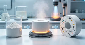
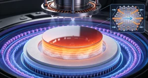
The manufacturing method is one of the most important differences between various BN grades. Pyrolytic boron nitride (PBN) is manufactured through a chemical vapor deposition process. Boron-containing and nitrogen-containing precursor gases react at elevated temperature, depositing BN layer by layer onto a substrate. This process allows extremely precise control over chemical composition and produces a highly dense structure. Because PBN does not rely on powder compaction or conventional sintering, it avoids many contamination sources associated with binders, additives, and residual pores. This makes PBN especially suitable for semiconductor environments where contamination tolerance is extremely low.
Hot-pressed BN (HPBN), on the other hand, is produced by consolidating BN powder under high temperature and pressure. The advantage of HPBN is its excellent machinability and flexibility in producing larger bulk components. However, the final purity and outgassing performance depend strongly on powder quality, densification level, and whether any additives are introduced during manufacturing.
The following table compares typical characteristics:
| Property | PBN | High-Purity HPBN |
|---|---|---|
| Manufacturing method | CVD deposition | Hot pressing |
| Typical purity | ≥99.99% | Grade dependent |
| Density | Very high, near fully dense | High depending on grade |
| Grain boundaries | Minimal | Present depending on structure |
| Outgassing performance | Excellent | Very good when properly processed |
| Machinability | More limited | Excellent |
| Complex bulk geometry | Limited | Excellent |
| Semiconductor vacuum application | Excellent | Suitable for qualified grades |
| Typical use | Crucibles, high-purity components | Fixtures, insulation, structural parts |
In boron nitride semiconductor manufacturing, the choice between PBN and HPBN is therefore not simply a comparison of purity values. Engineers must consider the actual location, thermal conditions, mechanical requirements, and contamination sensitivity of the component.
Controlling Impurity Levels in Semiconductor-Grade BN
Semiconductor processes are extremely sensitive to metallic contamination. Elements such as iron, sodium, potassium, calcium, copper, and other trace metals can influence electrical characteristics, carrier lifetime, or device reliability if introduced into sensitive regions. For this reason, semiconductor-grade BN requires strict control from raw material preparation through final inspection. High-purity BN materials are typically evaluated using analytical methods such as ICP-MS or other trace-element analysis techniques to verify impurity levels. The acceptable impurity level depends on the application. For example, a thermal insulation component inside a furnace may tolerate different impurity levels compared with a PBN crucible used for semiconductor crystal growth. Engineers should define purity requirements based on process sensitivity rather than applying the highest purity specification universally.
Surface contamination is another important factor. Even an ultra-high-purity BN component can create problems if it is contaminated during machining, handling, or storage. Fingerprints, dust particles, machining residues, and packaging materials can become sources of contamination during high-temperature operation. Therefore, semiconductor-grade BN manufacturing should include controlled machining, cleaning, inspection, and packaging procedures.
Low Outgassing Design Principles for Semiconductor-Grade Boron Nitride
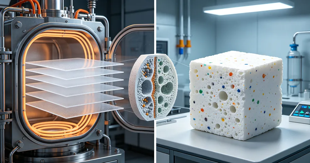
For semiconductor equipment engineers, low outgassing is not an independent material property; it is the result of material purity, microstructure, surface condition, and manufacturing control working together. A BN component may have excellent intrinsic chemical stability, but if it contains absorbed moisture, machining residues, excessive porosity, or surface contamination, its vacuum performance can still be affected. This is especially critical in deposition systems, molecular beam epitaxy (MBE), MOCVD, CVD, and other high-vacuum processes where even trace gas release can influence pressure stability and process repeatability. The first principle of achieving low outgassing is controlling the internal structure of the ceramic. Porosity is one of the most important factors because internal pores provide additional surfaces where water molecules and other contaminants can be physically absorbed. During vacuum heating, these trapped species gradually escape, increasing chamber pressure and potentially introducing unwanted elements into the process environment. Therefore, semiconductor-grade BN components should have high density, low open porosity, and stable microstructure.
Pyrolytic boron nitride (PBN) naturally has advantages in this area because the CVD deposition process produces a dense layered structure without conventional sintering additives. Research on PBN used for semiconductor processing has demonstrated its suitability due to its purity, thermal stability, and low contamination characteristics. Studies have reported that metallic impurity levels in high-quality PBN can be extremely low, while controlled vacuum baking can further reduce certain residual impurities. For hot-pressed BN, achieving low outgassing requires more attention to powder purity, densification conditions, and post-processing treatment. High-quality HPBN can provide excellent performance, but engineers must evaluate the specific grade rather than assuming all BN materials have identical vacuum behavior.
In boron nitride semiconductor manufacturing, low outgassing performance is particularly important because process contamination is cumulative. A component may release only a very small amount of gas during each thermal cycle, but repeated operation can gradually influence chamber conditions. For high-volume semiconductor production, stable performance over thousands of cycles is often more important than short-term material capability.
Thermal Treatment and Cleaning Before Semiconductor Use
A critical step in preparing BN components for semiconductor equipment is thermal conditioning or bake-out. Even high-purity BN can adsorb moisture or atmospheric molecules during storage and handling. Before installation into vacuum systems, controlled heating under vacuum or inert atmosphere can remove these physically absorbed species. The bake-out temperature and duration depend on the component geometry, BN grade, equipment limitation, and required vacuum level. Thin components generally release absorbed gases more quickly, while thick ceramic parts may require longer conditioning because gases trapped deeper inside the structure need more time to diffuse outward.
Cleaning procedures are equally important. Semiconductor-grade BN components should avoid contamination from conventional machining lubricants, oils, fingerprints, and workshop dust. Dry machining is often preferred for vacuum applications because organic residues from cutting fluids can become a source of carbon contamination during high-temperature operation. The surface condition after machining also affects outgassing. A rough or damaged surface may contain more adsorption sites compared with a carefully finished surface. For this reason, precision cleaning and controlled packaging are often considered part of the material specification rather than optional additional steps.
| Outgassing Control Method | Purpose | Engineering Effect |
|---|---|---|
| High-purity raw materials | Reduce metallic and chemical impurities | Lower contamination risk |
| Dense microstructure | Reduce trapped gases | Improve vacuum stability |
| Vacuum bake-out | Remove absorbed gases | Shorter pump-down time |
| Dry machining | Avoid organic residues | Reduce carbon contamination |
| Clean packaging | Prevent environmental contamination | Maintain surface purity |
| Controlled storage | Prevent moisture adsorption | Preserve vacuum performance |
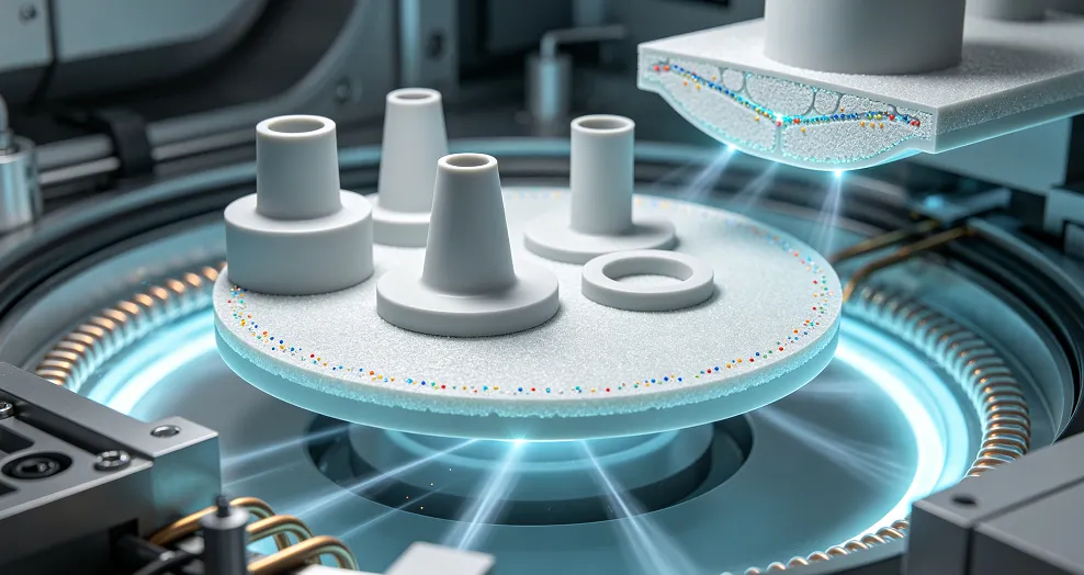
Purity Requirements for Semiconductor-Grade BN Components
Purity requirements for BN depend strongly on the application location. Semiconductor equipment contains many ceramic components, but not every component has the same contamination sensitivity. A BN crucible directly contacting semiconductor source material requires extremely high purity because any impurity released from the ceramic may directly enter the growing crystal or deposited film. A thermal shield or mechanical support located farther from the process zone may have different requirements.
The most important impurities considered in semiconductor applications are typically metallic elements such as iron, sodium, potassium, calcium, copper, and other transition metals. These elements can affect electrical properties, carrier concentration, or device reliability if transferred into sensitive semiconductor layers. For this reason, semiconductor-grade BN suppliers usually focus not only on total purity percentage but also on specific impurity analysis. A material labeled as “99.99% pure” does not automatically provide sufficient information for semiconductor qualification. Engineers need to understand what the remaining impurity fraction contains.
| Material Characteristic | Semiconductor Importance |
|---|---|
| Total purity | Indicates overall chemical cleanliness |
| Metallic impurity level | Prevents electrical contamination |
| Carbon content | Important for high-temperature vacuum processes |
| Density | Influences gas release behavior |
| Porosity | Determines adsorption capacity |
| Surface cleanliness | Controls particle and residue generation |
| Chemical stability | Prevents reaction with process materials |
In boron nitride semiconductor manufacturing, the material certificate and analytical data are often as important as the physical component itself. Engineers should evaluate purity according to process requirements rather than selecting the highest purity number without considering actual operating conditions.
Role of BN Flexible Materials in Semiconductor Thermal Protection
Not all semiconductor applications require rigid BN ceramics. Many systems require flexible insulation layers, separation materials, or protective barriers that must maintain purity while adapting to complex geometries. For example, Boron Nitride White Ring Paper can be used where a clean, high-temperature separation layer is required. Its role is not only mechanical separation but also maintaining a chemically stable interface between components during thermal processing. Because BN does not react easily with many high-temperature materials, it can help reduce sticking and contamination risks. Similarly, Boron Nitride Wrapping Paper provides flexible thermal protection for components that require insulation or surface protection during high-temperature operations. In semiconductor equipment, flexible BN materials can be useful where rigid ceramic parts cannot easily conform to the required shape. For electrical isolation applications, Boron Nitride Insulating Sleeve components provide high-temperature insulation while maintaining dimensional stability and chemical resistance. These components are often used around electrical connections or high-temperature structures where conventional polymer insulation cannot survive. The engineering value of these products comes from the same fundamental BN characteristics: chemical stability, low contamination potential, thermal resistance, and electrical insulation.
Designing BN Components for Ultra-Clean Semiconductor Environments
The design of semiconductor-grade BN components should consider the entire service environment, not only the material itself. A component that performs well in laboratory testing may behave differently when exposed to real manufacturing conditions involving repeated heating, vacuum cycling, plasma exposure, or reactive gases.
Engineers should evaluate several design factors:
| Design Factor | Why It Matters |
|---|---|
| Component location | Determines required purity level |
| Temperature profile | Influences gas release behavior |
| Vacuum level | Determines outgassing sensitivity |
| Contact material | Determines chemical compatibility |
| Thermal cycling frequency | Influences long-term stability |
| Surface finish | Affects adsorption and particle generation |
| Cleaning method | Influences contamination control |
For example, a BN insulating component installed close to a wafer may require a cleaner surface condition than a structural component located outside the process chamber. Similarly, a component exposed to repeated rapid heating cycles may require different mechanical considerations compared with a component operating at a stable temperature. The best semiconductor ceramic design approach is therefore application-specific. Material selection, machining, cleaning, and qualification should all be considered together.
Company Profile
JianXun Technology Co., Ltd. specializes in finished advanced ceramic components for semiconductor, high-temperature, thermal-processing, and electrical-insulation applications. The company provides Boron Nitride, Alumina, and Silicon Carbide ceramic products, including customized components designed according to technical drawings and application requirements. JianXun focuses on providing reliable ceramic solutions with controlled purity, thermal performance, electrical insulation, chemical stability, and dimensional accuracy for demanding industrial environments.
Payment Terms: T/T, PayPal, Credit Card, Western Union, or other agreed payment methods.
Shipment Terms: Products can be shipped by express, air freight, or sea freight according to product dimensions, quantity, and customer requirements.
Storage Conditions: Store ceramic components in a clean and dry environment. Keep products protected from moisture, dust, and contamination before installation.
FAQs
Q1: Why is low outgassing important for boron nitride used in semiconductor equipment?
Low outgassing is essential because semiconductor processes often operate under vacuum conditions where even small amounts of released gases can affect pressure stability, plasma behavior, deposition uniformity, and contamination control. BN components may appear chemically stable under normal conditions, but absorbed moisture, residual impurities, machining residues, and internal porosity can become sources of gas release when exposed to high temperature or vacuum. In boron nitride semiconductor manufacturing, engineers must evaluate not only the chemical composition of BN but also its density, surface condition, cleaning process, and thermal history to ensure stable long-term performance.
Q2: Is PBN better than HPBN for semiconductor applications requiring low outgassing?
PBN generally has advantages in ultra-high vacuum and contamination-sensitive applications because its CVD manufacturing process creates a dense structure with very high purity and minimal porosity. It is widely used for semiconductor crystal growth, MOCVD, MBE, and other applications where contamination control is critical. However, HPBN can also provide excellent low-outgassing performance when manufactured with high-purity raw materials, proper densification, and controlled processing. The correct choice depends on the component function, required purity level, geometry, and operating environment rather than simply selecting PBN for every application.
Q3: How can engineers verify the purity of semiconductor-grade boron nitride?
Engineers should request detailed material analysis rather than relying only on a nominal purity percentage. Important information includes metallic impurity levels, carbon content, density, porosity, and manufacturing process information. Analytical techniques such as trace-element analysis can help determine whether the material meets semiconductor requirements. For boron nitride semiconductor manufacturing, purity qualification should be connected with the actual process sensitivity because a component used near a wafer or source material requires stricter control than a general high-temperature insulation component.
Q4: Can machining affect the outgassing performance of BN components?
Yes. Although BN itself has excellent stability, machining can introduce contamination if improper methods are used. Cutting fluids, lubricants, dust, and handling residues may remain on the surface and later release gases during vacuum heating. Machining damage can also increase surface adsorption sites. Therefore, semiconductor-grade BN components should use controlled machining processes, appropriate cleaning procedures, and contamination-controlled packaging before installation. The machining stage is an important part of achieving reliable performance in boron nitride semiconductor manufacturing.
Q5: What BN components require the highest purity and lowest outgassing performance?
Components directly exposed to semiconductor materials or the most sensitive process regions usually require the highest purity and lowest outgassing characteristics. These include crucibles, source containers, wafer-facing components, and critical thermal-processing parts. Other components such as insulation layers, protective barriers, and mechanical supports may have different requirements. Products such as Boron Nitride White Ring Paper, Boron Nitride Wrapping Paper, and Boron Nitride Insulating Sleeve are selected according to their specific thermal, electrical, and contamination-control functions within the equipment design.