Advanced Technical Ceramics, Precision Alumina, Silicon Carbide, Crucible Parts



What Is the Difference Between Pyrolytic Boron Nitride (PBN) and Hot Pressed Boron Nitride (HPBN) in Chip Fabrication?
As semiconductor fabrication moves toward tighter process windows, higher operating temperatures, and stricter contamination control, ceramic components inside process equipment have become increasingly important. Materials used near wafers, epitaxial layers, heaters, plasma regions, or crystal-growth zones must simultaneously withstand thermal cycling, chemical exposure, electrical fields, and demanding dimensional requirements. This is why boron nitride semiconductor manufacturing applications increasingly involve different BN grades rather than treating boron nitride as a single universal material.
Among the available BN technologies, Pyrolytic Boron Nitride (PBN) and Hot Pressed Boron Nitride (HPBN) are particularly important. Both are based primarily on hexagonal boron nitride (h-BN), but they are manufactured through fundamentally different routes. PBN is formed through chemical vapor deposition, while HPBN is produced by consolidating BN powder under elevated temperature and pressure. The resulting differences in microstructure, purity, anisotropy, density, machining behavior, and vacuum performance determine where each material is technically appropriate. For an engineer, the question is therefore not simply whether PBN is “better” than HPBN. The more useful question is: Which manufacturing route produces the material characteristics required by a particular semiconductor process? That distinction is critical when designing or replacing furnace components, thermal-processing fixtures, insulation structures, crucibles, carriers, and other precision ceramic parts.
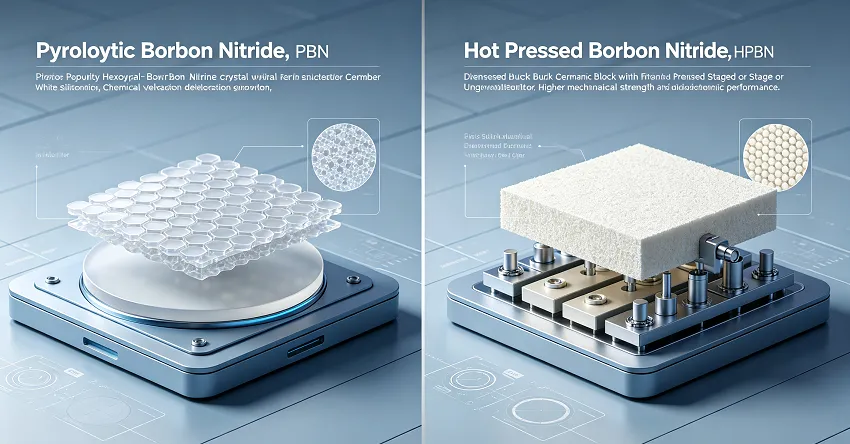
I. PBN and HPBN: The Manufacturing Route Determines the Material
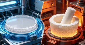
Pyrolytic Boron Nitride is manufactured by depositing BN from a gaseous phase onto a heated substrate. During the CVD process, boron- and nitrogen-containing precursors react at elevated temperature and form successive layers of BN. The deposition conditions can be tightly controlled, producing a dense, highly oriented material with very low impurity levels. Unlike conventional powder-based ceramics, PBN does not depend on conventional sintering additives or binders to create its primary structure. This manufacturing mechanism is one of the reasons PBN is valuable in boron nitride semiconductor manufacturing. When a BN component is positioned directly inside a highly sensitive process environment, purity and low outgassing can be more important than mechanical strength or machining convenience. PBN’s dense structure and controlled composition make it particularly attractive for semiconductor crystal growth, epitaxial processing, and other applications where contamination from the process hardware must be minimized.
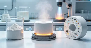
HPBN follows a fundamentally different route. High-purity BN powder is shaped and consolidated using heat and pressure. The resulting bulk ceramic is generally polycrystalline, with properties influenced by powder characteristics, forming pressure, temperature, densification, porosity, and the degree of platelet orientation developed during processing. Because HPBN starts from a bulk powder body, manufacturers can produce relatively large plates, rings, blocks, tubes, and other shapes that can subsequently be machined to engineering drawings. This difference gives HPBN an important advantage in boron nitride semiconductor manufacturing equipment design. Engineers can specify holes, slots, grooves, stepped geometries, mounting features, and other details that would be difficult or uneconomical to achieve with a deposited PBN structure. HPBN is therefore often selected when the component is mechanically integrated into a larger furnace or process assembly rather than directly exposed to the most contamination-sensitive semiconductor region.
II. PBN vs HPBN: Engineering Performance Comparison
The two materials should be compared according to the actual component function rather than by looking at a single property. Typical values vary considerably with grade, processing conditions, orientation, and supplier, so the following table should be treated as an engineering comparison rather than a universal material specification.
| Property | Pyrolytic Boron Nitride (PBN) | Hot Pressed Boron Nitride (HPBN) |
|---|---|---|
| Primary Manufacturing Route | Chemical Vapor Deposition (CVD) | Hot pressing of BN powder |
| Material Structure | Highly oriented layered structure | Polycrystalline, partially oriented structure |
| Typical Purity | Often ≥99.99% for high-purity grades | Commonly 99–99.9%, depending on grade |
| Typical Density | Approximately 2.1–2.2 g/cm³ | Approximately 1.8–2.1 g/cm³ |
| Porosity | Extremely low | Depends on densification and grade |
| Thermal Conductivity | High, strongly direction-dependent | Moderate to high, also orientation-dependent |
| Electrical Resistivity | Very high | Very high |
| Dielectric Performance | Excellent | Excellent |
| Thermal Shock Resistance | Excellent | Excellent |
| Chemical Stability | Excellent in suitable atmospheres | Excellent in suitable atmospheres |
| Vacuum Compatibility | Excellent | Good to excellent depending on grade and processing |
| Outgassing | Very low | Generally higher than PBN |
| Machinability | Relatively difficult | Excellent compared with PBN |
| Complex Geometry | More difficult and costly | Highly suitable |
| Large Structural Components | More limited | Generally more practical |
| Typical Semiconductor Uses | MOCVD, crystal growth, crucibles, liners | Furnace fixtures, insulation parts, shields, custom components |
| Main Engineering Advantage | Purity and process cleanliness | Machinability and structural flexibility |
The table also highlights an important point: boron nitride semiconductor manufacturing does not automatically mean that every semiconductor component should use PBN. Semiconductor equipment contains many different component zones. A component directly contacting a growing crystal may require the purity characteristics of PBN, while a support bracket or thermal shield located farther from the process zone may benefit more from the machinability and structural flexibility of HPBN.
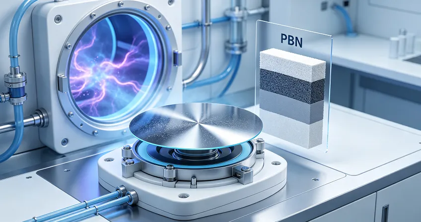
III. Why PBN Is Preferred for Ultra-Clean Semiconductor Processes
PBN becomes particularly attractive when the ceramic itself is part of the contamination-control strategy. Semiconductor crystal growth and epitaxial processes can be extremely sensitive to metallic impurities and volatile species released from surrounding components. A material may have excellent thermal properties and still be unsuitable if it introduces contaminants into the process chamber. The CVD route used to produce PBN enables very high material purity and a dense microstructure. PBN can therefore be used for crucibles, liners, susceptors, boats, and other components in demanding high-temperature environments. Its chemical stability and low outgassing characteristics are also valuable under vacuum or controlled-atmosphere conditions.
Another important characteristic is its layered structure. PBN exhibits strong anisotropy because the BN layers have a preferred orientation. Thermal conductivity and thermal expansion therefore cannot always be represented accurately by one isotropic value. In boron nitride semiconductor manufacturing, this becomes important when designing components that experience directional heat flow. An engineer must know whether heat travels parallel or perpendicular to the deposited layers because the thermal response can differ substantially. PBN is not, however, automatically the best choice when complicated geometry is required. Its deposition-based manufacturing process can make large, thick, or intricately shaped components difficult to produce economically. Machining also needs to be carefully controlled because the material structure is highly oriented. Consequently, PBN is generally selected where its purity and process performance provide a meaningful technical benefit.
IV. Why HPBN Is More Practical for Precision-Machined Components
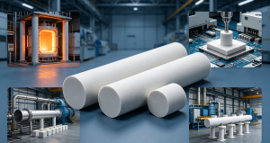
HPBN offers a different engineering value proposition. Its powder-based manufacturing route makes it possible to produce bulk ceramic shapes that can be precision-machined after densification. This is particularly useful when a semiconductor equipment component must integrate with heaters, supports, shields, electrodes, or other mechanical assemblies. In boron nitride semiconductor manufacturing, HPBN can be used for insulation rings, plates, spacers, furnace fixtures, thermal shields, and customized structural parts. The engineer can design the component around the equipment rather than being restricted to the geometry naturally available from a deposition process.
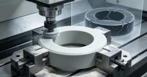
Machinability is particularly valuable during equipment development. Semiconductor tools frequently undergo design modifications, and ceramic components may require changes in hole location, thickness, clearance, or mounting geometry. HPBN allows these modifications to be implemented more readily than PBN, reducing the manufacturing burden associated with customized components. However, HPBN should not be evaluated only from the perspective of machining. Density, porosity, purity, grain orientation, and manufacturing consistency remain important. A poorly controlled HPBN grade may not be appropriate for a highly sensitive semiconductor chamber even if its dimensional accuracy is excellent. Material selection must therefore consider both the component’s mechanical role and its proximity to the active process region.
V. How Engineers Should Choose PBN or HPBN
The most reliable selection method begins with the operating environment. If the component directly contacts a semiconductor crystal, epitaxial material, or highly sensitive process environment, purity and outgassing should be among the first criteria. Under these circumstances, PBN often has a technical advantage. If the component primarily provides mechanical support, electrical isolation, thermal shielding, or positioning, HPBN may offer a better balance of performance and manufacturing flexibility. In boron nitride semiconductor manufacturing, the distinction between process-critical and equipment-support components is therefore extremely useful.
Temperature and atmosphere must also be evaluated together. BN generally performs very well at elevated temperatures under vacuum or inert atmospheres, but its behavior changes in oxidizing environments. Engineers should therefore specify not only the maximum temperature but also the actual atmosphere, pressure, exposure duration, and thermal-cycle frequency. Component geometry is another decisive factor. A simple PBN tube or plate may be technically attractive when purity is critical, whereas a complex machined ring with multiple holes and mounting surfaces may be better manufactured from HPBN. Mechanical loading, dimensional tolerance, surface finish, and thermal gradients should then be incorporated into the final selection.
VI. Where BN Paper Products Fit Into Semiconductor and High-Temperature Processing
Not every BN application requires a rigid ceramic component. Thin BN materials can provide separation, release, insulation, and surface-protection functions while introducing very little additional thickness into a thermal assembly.
Boron Nitride Release Paper is particularly useful where a high-temperature process requires controlled separation between a ceramic product and its supporting surface. The low reactivity of BN helps reduce adhesion and facilitates removal after thermal processing. From an engineering standpoint, the value of release paper is not simply its ability to “release”; thickness, surface cleanliness, thermal stability, flexibility, and compatibility with the surrounding process must all be considered.
Boron Nitride White Ring Paper is suited to applications requiring a thin BN-based separation or insulation layer around ring-shaped or localized process structures. Its function can be particularly relevant where direct contact between different components must be minimized without introducing a thick rigid ceramic spacer.
Boron Nitride Wrapping Paper provides a flexible BN-based protective layer for thermal insulation and high-temperature separation. Compared with rigid HPBN components, paper-form BN can conform to surfaces and accommodate assembly conditions where dimensional flexibility is more important than structural rigidity.
These products broaden the role of BN in boron nitride semiconductor manufacturing. The engineer can select between a deposited PBN component, a machined HPBN component, or a flexible BN paper depending on whether the primary requirement is ultra-high purity, structural support, electrical insulation, thermal separation, or release behavior.
VII. PBN and HPBN: What Matters During Supplier Evaluation?
For technical purchasing, comparing only “PBN” and “HPBN” on a quotation is not sufficient. The supplier should be able to provide the material grade, manufacturing method, purity level, density, dimensional tolerances, and relevant thermal and electrical data. For anisotropic BN, the direction in which thermal conductivity was measured should also be identified. In boron nitride semiconductor manufacturing, batch consistency is particularly important. A component that meets a nominal density specification but exhibits large variations in porosity or impurity content may behave differently from batch to batch. Engineers should therefore pay attention to quality-control procedures, dimensional inspection, surface treatment, packaging cleanliness, and traceability.
For PBN, the engineer should additionally consider deposition orientation, wall thickness, purity, surface condition, and thermal cycling history. For HPBN, density, porosity, machining quality, purity, and orientation should receive greater attention. The material certificate should correspond to the actual production grade rather than a generic BN specification.
VIII. JianXun Technology Co., Ltd.
JianXun Technology Co., Ltd. provides finished advanced ceramic components for demanding thermal, electrical, chemical, and precision industrial applications. Its product range includes boron nitride, alumina, aluminum nitride, silicon carbide, and customized ceramic components designed according to application-specific requirements.
For boron nitride semiconductor manufacturing, material selection should be based on the actual operating environment rather than a generic BN specification. JianXun can support customized BN products according to component geometry, temperature, atmosphere, electrical insulation requirements, dimensional tolerances, and application conditions. The product range can include rigid BN plates, rings, gaskets, insulation components, and BN paper products for high-temperature processing and separation applications.
IX.FAQs
Q1: Is PBN always better than HPBN for semiconductor manufacturing?
No. PBN is not universally superior to HPBN; the appropriate material depends on the component’s function, process environment, and required performance window. PBN offers significant advantages when ultra-high purity, low outgassing, chemical stability, and contamination control are critical. These characteristics make it particularly suitable for components positioned close to semiconductor crystal-growth or epitaxial regions, where even trace impurities from process hardware may affect material quality. However, PBN becomes less attractive when the component requires complicated machining, large dimensions, multiple mounting features, or cost-effective customization. HPBN provides a different combination of properties. Its powder-based manufacturing route allows engineers to produce bulk ceramic components and machine them into complex geometries with relatively tight dimensional tolerances. For furnace fixtures, insulating rings, thermal shields, spacers, and other equipment components that do not directly contact the most contamination-sensitive process material, HPBN can provide a more practical balance between thermal stability, electrical insulation, machinability, and manufacturing cost. Therefore, in boron nitride semiconductor manufacturing, engineers should select PBN or HPBN according to the actual operating conditions rather than assuming that the material with the highest purity is automatically the best solution.
Q2: Why does PBN generally have higher purity than HPBN?
The difference in purity is primarily related to how the two materials are manufactured. PBN is produced through a Chemical Vapor Deposition process, in which boron nitride is deposited from gaseous precursors onto a heated substrate. Because the material is built layer by layer from the vapor phase, the deposition environment and chemical composition can be tightly controlled. This makes it possible to produce extremely high-purity BN with a dense structure and very low levels of unwanted metallic or other impurities. HPBN is manufactured from BN powder through forming and hot pressing. Although high-purity BN powders can be used, the final ceramic is still influenced by powder purity, processing conditions, densification, handling, and machining. Its performance therefore depends not only on the nominal purity of the starting powder but also on the complete manufacturing process. In boron nitride semiconductor manufacturing, this distinction becomes particularly important for components located directly inside sensitive process zones. When contamination control is the dominant requirement, PBN may provide a greater material margin. When the component performs a structural or insulating function away from the most sensitive region, a properly specified high-purity HPBN grade may be sufficient.
Q3: Can HPBN be used inside vacuum semiconductor equipment?
Yes, HPBN can be used in vacuum and controlled-atmosphere semiconductor equipment, but the material grade and manufacturing quality must be evaluated carefully. Engineers should consider purity, density, open porosity, surface condition, machining residues, outgassing behavior, and the temperature at which the component will operate. Simply specifying “HPBN” does not provide enough information to determine whether a particular grade is suitable for a high-vacuum system. For boron nitride semiconductor manufacturing, vacuum compatibility is particularly important because gases released from ceramic components can alter chamber conditions and potentially affect process stability. Dense, high-purity HPBN with controlled porosity and appropriate post-machining cleaning can be suitable for many equipment applications. However, when the component is positioned extremely close to the active wafer or crystal-growth zone, or when the process has exceptionally strict contamination requirements, PBN may offer additional advantages because of its dense CVD-derived structure and very high purity. The engineer should therefore evaluate the complete vacuum system rather than focusing only on the BN material name. Component location, chamber pressure, operating temperature, exposure time, thermal cycling, and cleaning procedures all influence actual vacuum performance.
Q4: Why is PBN commonly used for MOCVD and semiconductor crystal-growth applications?
PBN is particularly attractive for MOCVD and semiconductor crystal-growth equipment because these processes combine high temperature with stringent requirements for material purity, chemical stability, and process cleanliness. Components such as crucibles, liners, susceptors, and other process fixtures may be exposed directly to reactive gases or positioned very close to the material being deposited or grown. Under these conditions, the ceramic component itself becomes part of the process environment and must not introduce significant contamination.
The CVD manufacturing route gives PBN a highly dense and oriented structure with very high purity. It also provides excellent resistance to many high-temperature process environments when the atmosphere is properly controlled. In boron nitride semiconductor manufacturing, these characteristics help maintain a stable process environment while reducing the risk that the equipment material will interfere with crystal growth or epitaxial deposition. Another consideration is thermal behavior. PBN has a layered structure that produces anisotropic thermal properties, so engineers must understand the orientation of the material when designing components exposed to strong thermal gradients. For crystal-growth equipment, thermal uniformity can influence the growth environment, making the relationship between PBN orientation, geometry, heater configuration, and heat flow an important part of component design.
Q5: How should engineers decide whether a customized PBN or HPBN component is suitable for their semiconductor equipment?
Engineers should begin with the actual operating conditions rather than the component name. The specification should identify operating temperature, atmosphere, pressure or vacuum level, thermal-cycle frequency, mechanical loading, electrical requirements, dimensional tolerances, surface finish, purity requirements, and whether the ceramic directly contacts the wafer, crystal, precursor gases, or other process materials. These parameters determine whether the priority should be ultra-high purity, thermal performance, mechanical strength, machinability, or a combination of these properties. For boron nitride semiconductor manufacturing, component geometry is equally important. A relatively simple crucible or liner exposed directly to a sensitive process may justify PBN because purity and vacuum performance are dominant requirements. A complex furnace fixture with multiple holes, slots, steps, or mounting surfaces may be better suited to HPBN because machining flexibility becomes a major engineering advantage. Thermal conductivity should also be evaluated according to the actual heat-flow direction because both PBN and HPBN can exhibit anisotropic thermal behavior. The supplier should ideally receive a detailed engineering drawing together with the operating conditions rather than only a material name such as “PBN” or “HPBN.” A technically complete specification should also identify the required purity level, density range, dimensional tolerance, surface condition, inspection requirements, and intended service environment. This allows the BN component to be selected according to its actual function within the equipment, reducing the risk of choosing an unnecessarily expensive material or, conversely, using a ceramic grade that does not provide sufficient process stability.