Advanced Technical Ceramics, Precision Alumina, Silicon Carbide, Crucible Parts



Which Boron Nitride Grade Is Best for MOCVD/CVD Crucibles and Wafer Applications?
In semiconductor processing, asking which boron nitride grade is “best” for MOCVD/CVD crucibles or wafer-related components is not simply a question of selecting the highest-purity BN available. The correct engineering choice depends on the process atmosphere, temperature profile, precursor chemistry, contamination tolerance, thermal uniformity, component geometry, mechanical loading, and the required service lifetime. Among the major boron nitride families, Pyrolytic Boron Nitride (PBN) is generally the preferred grade when the component directly participates in a high-purity vacuum, epitaxial growth, crystal-growth, or source-containment process, while high-purity hot-pressed BN (HPBN) remains highly useful for larger, machinable insulating and structural components. This distinction is particularly important in boron nitride semiconductor manufacturing, where a ceramic component is not merely a passive heat-resistant part: its surface chemistry, impurity level, gas permeability, thermal anisotropy, and interaction with process gases can influence contamination, temperature uniformity, and ultimately process stability.
I. Why the “Best” Boron Nitride Grade Depends on the Process
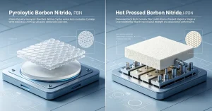
For engineers working on MOCVD and CVD equipment, the first mistake is to treat all hexagonal boron nitride as equivalent. Conventional hot-pressed BN, high-purity HPBN, PBN, and other engineered BN grades share the basic h-BN crystal chemistry, but their manufacturing routes create very different microstructures. HPBN is consolidated from BN powder under high temperature and pressure, whereas PBN is deposited directly from gaseous precursors through a CVD process. The latter produces a dense, layered structure in which the BN crystallites are preferentially oriented parallel to the deposition surface. This structure is one reason PBN can provide exceptionally high purity and excellent gas-barrier characteristics, but it also introduces strong anisotropy in thermal and mechanical properties. In practical boron nitride semiconductor manufacturing, therefore, material selection should begin with the function of the component rather than simply its nominal BN purity.
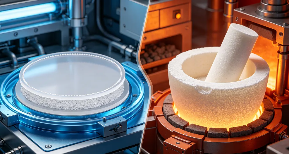
For a crucible that holds semiconductor source material, precursor-related materials, or other contamination-sensitive substances, the material is directly exposed to the process environment. Here, purity and surface condition become critical. A PBN crucible can provide a dense, smooth, chemically stable containment surface with very low impurity contribution compared with many conventional sintered ceramic alternatives. This is why PBN crucibles are widely associated with compound-semiconductor crystal growth, MBE, MOCVD/CVD equipment, and high-vacuum evaporation applications. By contrast, HPBN becomes more attractive when the engineer needs a thicker, mechanically robust, easily machined bulk component rather than an ultra-thin, highly dense deposited structure.
II. PBN, HPBN and Other BN Grades: What Actually Changes?
The fundamental difference between PBN and HPBN is not simply purity; it is how the material is made and what microstructure that manufacturing process creates. HPBN begins with h-BN powder. The powder is compacted and densified through hot pressing or related high-temperature consolidation methods. Depending on the grade and formulation, additives or sintering aids may be involved, although high-purity semiconductor-oriented grades are engineered to minimize undesirable contamination. Because HPBN is produced as a bulk ceramic, engineers can obtain relatively thick plates, blocks, rings, tubes, supports, and machined geometries. This makes HPBN attractive for equipment components where dimensional stability and machinability are more important than achieving the absolute lowest impurity level.
PBN follows a completely different route. High-purity gaseous boron- and nitrogen-containing precursors react at elevated temperature and deposit BN directly onto a substrate or mandrel. Because the material is built layer by layer rather than consolidated from powder, the resulting structure can be exceptionally dense and uniform. Commercial PBN commonly reaches 99.99% purity, with higher-purity grades available for particularly contamination-sensitive applications. The CVD-derived structure also explains why PBN is normally supplied in relatively thin walls and why its thermal conductivity is highly directional. In boron nitride semiconductor manufacturing, this combination of purity, density, chemical stability, and anisotropic heat transfer is particularly valuable when designing crucibles and other components that must maintain a controlled thermal environment.
Technical Comparison of Major BN Grades
| Parameter | Standard HPBN | High-Purity HPBN | PBN | Engineering Significance |
|---|---|---|---|---|
| Manufacturing route | Hot pressing / powder consolidation | High-purity hot pressing | CVD deposition | Determines microstructure and impurity profile |
| Typical purity | Grade dependent | Typically higher than standard HPBN | Commonly ≥99.99% | Important for contamination-sensitive processes |
| Microstructure | Bulk polycrystalline | Refined bulk polycrystalline | Layered, highly oriented | Strongly affects thermal/mechanical anisotropy |
| Density | Grade dependent | Generally high | High and uniform | Influences gas permeability and surface integrity |
| Thermal conductivity | Direction-dependent | Direction-dependent | Strongly anisotropic | Important for temperature uniformity |
| Machinability | Good | Good | More limited | HPBN is easier for complex bulk geometries |
| Thin-wall capability | Good | Good | Excellent for deposited structures | Important for crucibles and thermal components |
| Vacuum compatibility | Grade dependent | Good when properly processed | Excellent for suitable grades | Depends on density, cleaning and outgassing |
| Chemical stability | Excellent | Excellent | Excellent | Important under aggressive process conditions |
| Typical role | Structural/insulating components | Semiconductor equipment components | High-purity crucibles and critical surfaces | Selection depends on process function |
The values in such a table should always be treated as grade- and manufacturer-dependent, rather than universal material constants. For example, published PBN data show substantial directional differences in thermal conductivity, with representative values around tens of W/m·K in the basal plane and only a few W/m·K through the thickness. That anisotropy is not a defect; it is an intrinsic consequence of the PBN layered structure and can actually be exploited in crucible design.
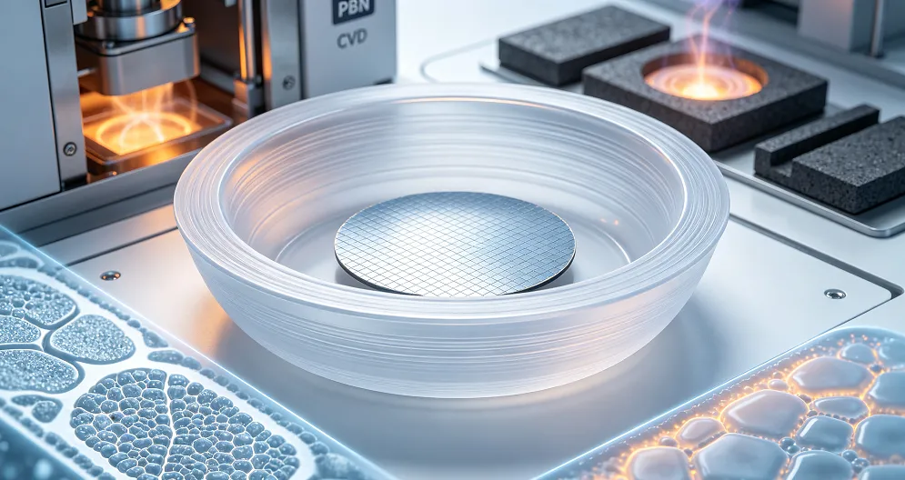
III. Why PBN Is Usually the First Choice for MOCVD and CVD Crucibles
For a true semiconductor-process crucible, PBN is often the engineering starting point because the crucible itself can become part of the contamination budget. During high-temperature processing, trace metallic impurities, oxygen-containing species, adsorbed moisture, volatile compounds, and particles released from the equipment can migrate into the process environment. If the crucible is used for compound-semiconductor source materials or crystal growth, even a relatively small impurity contribution can become significant over repeated thermal cycles. PBN addresses this problem through its CVD-derived purity and dense surface structure. Several suppliers specifically identify PBN crucibles for GaAs, InP and other III-V compound-semiconductor crystal-growth processes as well as MOCVD and CVD equipment.
The second advantage is chemical behavior. Hexagonal BN is chemically stable over a broad range of processing environments and is generally non-wetting toward many molten materials. For semiconductor processing, this is important because the crucible should contain the source material without becoming a reactive participant. A crucible that reacts with its charge, develops a reaction layer, or releases contaminants after repeated heating can create process drift. PBN therefore fits applications where the engineer needs a clean, chemically stable interface rather than merely a ceramic capable of surviving a high nominal temperature. In boron nitride semiconductor manufacturing, this distinction between “temperature resistant” and “process compatible” is fundamental.
Thermal behavior is equally important. PBN’s in-plane thermal conductivity is considerably higher than its through-thickness conductivity, meaning that heat can spread efficiently along the deposited layers while heat transfer across the wall remains comparatively restricted. Shin-Etsu, for example, describes PBN crucibles as taking advantage of high in-plane thermal conductivity and thermal insulation through the thickness. This can help establish a predictable thermal field around the material being processed. For crystal growth and vapor-phase processes, thermal uniformity is often more important than simply maximizing thermal conductivity.
IV. What PBN Grade Should Be Selected for MOCVD/CVD?
For most contamination-sensitive MOCVD/CVD applications, a high-purity PBN grade, normally starting around 4N purity and moving toward 5N or an application-specific ultra-high-purity specification when the process requires it, is the most logical choice. However, purity alone should never be the purchasing specification. An engineer should request the impurity profile, density, dimensional tolerances, wall thickness, surface condition, gas permeability or vacuum-performance data where relevant, thermal-property orientation, and cleaning/handling requirements. A supplier that only states “99.99% BN” without explaining what impurities remain may not be providing enough information for a serious semiconductor process qualification.
The distinction becomes especially important for GaN-related MOCVD systems. Gallium nitride epitaxy involves elevated temperatures and reactive precursor chemistry, and the equipment environment must maintain stable thermal and chemical conditions. PBN can be useful in components where the material must withstand the process without introducing significant contamination. Nevertheless, not every MOCVD component should automatically be made from PBN. Large structural supports, thermal shields, insulating fixtures, and mechanically demanding components may benefit more from engineered HPBN because their dominant requirement is dimensional stability, mechanical strength, machinability, or cost-effective replacement rather than direct source containment. Thus, the correct boron nitride semiconductor manufacturing strategy is often a combination of PBN and HPBN rather than a single BN grade throughout the entire chamber.
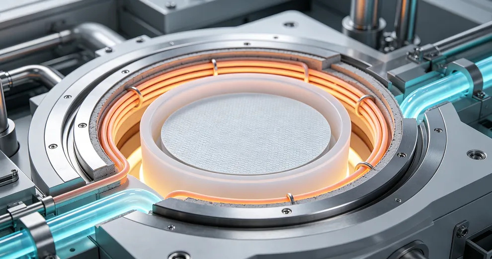
V. What About Wafer Applications?
“Wafer application” requires even more careful definition because the wafer itself may not be made from BN. In semiconductor equipment, BN can instead appear as a wafer support, carrier, insulation component, susceptor-related structure, spacer, shield, ring, or other component positioned close to the wafer. The engineering requirement is therefore to control the local environment around the wafer without introducing particles, metallic contamination, excessive thermal gradients, or unwanted electrical effects.
For these applications, the choice between PBN and HPBN depends heavily on whether the BN component directly faces the process zone. A PBN surface can be advantageous when extremely high purity, dense surface structure, and low contamination risk are required. Its thin-wall capability and highly uniform deposited surface can also be useful for specialized components with controlled geometry. However, if the wafer-support component is thick, mechanically loaded, repeatedly machined, or geometrically complex, high-purity HPBN can be more practical. The engineer should evaluate not only the ceramic itself but also machining damage, edge quality, cleaning procedures, thermal expansion mismatch, and the possibility of particle generation during thermal cycling.
This is particularly relevant to boron nitride semiconductor manufacturing because wafer-level contamination is not simply determined by the nominal chemical purity of the ceramic. A theoretically ultra-high-purity material can still cause problems if it has poor dimensional control, damaged machining surfaces, unstable coatings, improper cleaning, or thermal stresses that generate particles. In other words, “5N” does not automatically mean “best wafer material.” Process qualification must consider the entire component lifecycle.
VI. PBN vs HPBN for Wafer-Adjacent Components
| Engineering Requirement | PBN | High-Purity HPBN | Preferred Direction |
|---|---|---|---|
| Ultra-high chemical purity | Excellent | Very good to excellent, grade dependent | PBN |
| Dense, low-permeability surface | Excellent | Good to very good | PBN |
| Complex machined geometry | Moderate | Excellent | HPBN |
| Thick structural component | Limited by deposition economics/geometry | Excellent | HPBN |
| Thin-wall component | Excellent | Good | PBN |
| Thermal anisotropy control | Strong | Moderate/grade dependent | Depends on design |
| Large component cost efficiency | Lower | Generally better | HPBN |
| Direct contamination-sensitive interface | Excellent | Grade dependent | PBN |
| Mechanical robustness in bulk geometry | Good but geometry dependent | Very good | HPBN |
| Vacuum process suitability | Excellent for qualified grades | Good to excellent for qualified grades | Process dependent |
The practical result is that PBN is usually the stronger candidate for the most contamination-sensitive interface, whereas HPBN is often the stronger candidate for the most mechanically demanding bulk structure. This is one of the most important distinctions engineers should make before selecting a BN grade.
VII. When HPBN Is Actually Better Than PBN
There is a tendency in semiconductor marketing to describe PBN as the premium solution and therefore assume it must be superior in every application. That is not technically correct. PBN is expensive because the CVD manufacturing process is slow and geometry-dependent, and its layered microstructure imposes design constraints. For a thick support, large insulating block, mechanically loaded fixture, or component requiring extensive machining, HPBN can provide a much more rational engineering solution.
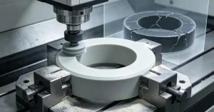
HPBN is especially attractive when the component needs holes, slots, steps, threads, complex mounting surfaces, or other machined features. Because the material exists as a bulk ceramic before machining, designers can work with substantially greater geometric freedom than is practical with thin PBN deposition. This matters in boron nitride semiconductor manufacturing because semiconductor equipment contains many components that do not directly contact the wafer or process source but still require electrical insulation, thermal stability, chemical resistance, and dimensional precision.
A well-selected high-purity HPBN can therefore be used for supports, spacers, insulating structures, furnace fixtures, thermal shields, rings, and other equipment components where the contamination risk is manageable. The important point is to specify the grade according to the actual process environment rather than assuming that every BN component needs PBN-level purity.
VIII. BN Components Beyond Crucibles and Wafer Carriers
A semiconductor thermal-processing system normally contains many BN components beyond the main crucible or wafer-support structure. Electrical insulation, thermal isolation, gas-flow protection, mechanical positioning, and local heat management all require ceramics with different combinations of properties. For example, an insulating component may prioritize high electrical resistivity and dimensional stability, while a nozzle may prioritize chemical stability, thermal shock resistance, and controlled geometry.
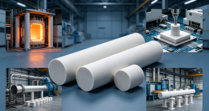
For applications requiring electrical isolation in high-temperature environments, a Boron Nitride Insulating Sleeve can be used where metallic components would create unwanted electrical paths or where conventional oxide ceramics cannot provide the required combination of thermal and chemical performance. Likewise, a BN Nozzle can be selected for controlled gas or material delivery where the component must maintain dimensional stability under thermal cycling. A BN Rod can serve as a support or insulating structural element in high-temperature equipment. These components demonstrate why BN selection should be approached as a system-level engineering exercise rather than simply a search for the “highest purity” material.
In boron nitride semiconductor manufacturing, the correct specification for these secondary components can sometimes be more important than increasing the nominal purity by another fraction of a percent. A poorly designed support can distort during thermal cycling, a nozzle can alter process flow because of dimensional changes, and an insulating sleeve can fail because of mechanical stress or improper thermal expansion matching. Therefore, engineers should evaluate purity, density, thermal conductivity, CTE, dielectric properties, surface finish, machining tolerance, and operating atmosphere together.
IX. Recommended Selection Logic for Engineers
The selection process can be reduced to several engineering decisions. If the component directly contains a semiconductor source, is used in high-vacuum crystal growth, or presents a highly contamination-sensitive surface to the process, PBN should normally be evaluated first. If the component is a thin-wall crucible or specialized high-purity vessel, PBN is again a strong candidate. If the component must be thick, mechanically robust, heavily machined, or produced in a complex three-dimensional geometry, high-purity HPBN deserves serious consideration.
The next step is to define the atmosphere. BN behaves very differently in vacuum, inert gas, nitrogen, hydrogen-containing environments, and oxidizing atmospheres. Published maximum-temperature values should never be copied directly into a design specification without identifying the atmosphere and exposure time. Many BN grades tolerate extremely high temperatures under inert or vacuum conditions, while oxidation becomes a much stronger limitation in air. For boron nitride semiconductor manufacturing, this means that “maximum temperature” should always be written together with atmosphere, pressure, duty cycle, and expected thermal cycling.
Finally, engineers should evaluate the component after processing rather than only when new. A crucible that performs perfectly for the first ten cycles but accumulates deposits, reacts with the source material, develops cracks, or becomes difficult to clean may be inferior to a slightly more expensive grade with a longer qualified lifetime. Semiconductor equipment should therefore evaluate BN according to contamination control + thermal behavior + mechanical reliability + cleanability + lifetime, not according to material price alone.
X. Practical PBN vs HPBN Selection Matrix
| Application | Recommended BN Grade | Main Reason | Key Engineering Check |
|---|---|---|---|
| MOCVD/CVD high-purity crucible | High-purity PBN | Purity and dense CVD structure | Impurity profile, wall thickness, thermal uniformity |
| III-V crystal-growth crucible | PBN | Chemical stability and high purity | Material compatibility and thermal cycling |
| MBE source crucible | PBN | Vacuum compatibility and low contamination | Outgassing, surface condition |
| Wafer-adjacent high-purity component | PBN / high-purity HPBN | Depends on contamination sensitivity | Particle generation and cleaning |
| Large thermal shield | HPBN | Bulk geometry and machinability | Density, strength, thermal cycling |
| Insulating sleeve | High-purity HPBN or PBN | Electrical and thermal isolation | CTE, resistivity, dimensional tolerance |
| BN nozzle | HPBN / PBN | Depends on process chemistry and geometry | Wear, thermal shock, internal surface |
| BN support rod | HPBN | Structural machinability | Flexural strength and thermal expansion |
| Complex machined fixture | HPBN | Geometric flexibility | Machining quality and particle control |
XI. FAQs
Q1: Is PBN always better than HPBN for semiconductor manufacturing?
No. PBN is generally the preferred choice when ultra-high purity, dense surface structure, vacuum compatibility, and contamination control dominate the engineering requirements, particularly for crucibles and other critical interfaces. HPBN can be the better material when the component is large, thick, mechanically loaded, or geometrically complex because its bulk structure is much easier to machine and manufacture economically. In boron nitride semiconductor manufacturing, the right question is therefore not “Which material is more advanced?” but “Which microstructure and manufacturing route provide the required performance at the specific location inside the equipment?” A PBN crucible may be the correct choice while an HPBN support surrounding that crucible is simultaneously the better engineering solution.
Q2: What PBN purity should be specified for MOCVD and CVD crucibles?
A 99.99% PBN grade is a common starting point for high-purity applications, while 99.999% or application-specific ultra-high-purity grades may be appropriate when the contamination budget is particularly restrictive. However, the purity percentage by itself is insufficient as a semiconductor specification. Engineers should request an impurity analysis, especially for metallic elements that could enter the process, together with density, surface condition, dimensional tolerance, and relevant vacuum or outgassing information. In boron nitride semiconductor manufacturing, the remaining impurity species can matter more than the difference between two nominal purity labels, so a material certificate or analytical report is much more useful than simply specifying “high-purity BN.”
Q3: Can HPBN be used in MOCVD/CVD equipment instead of PBN?
Yes, provided that the specific HPBN grade is qualified for the process location and contamination requirements. HPBN can be very useful for insulation, support structures, thermal shields, rings, spacers, and other components that do not require the same ultra-high-purity interface as a PBN source crucible. The engineer should examine the HPBN manufacturing route, additive or impurity content, density, porosity, surface finish, machining condition, and behavior under the actual process atmosphere. In boron nitride semiconductor manufacturing, using HPBN selectively can actually improve equipment economics without compromising process performance, provided that it is kept away from locations where its impurity profile or surface characteristics could affect the wafer or source material.
Q4: Why is PBN particularly suitable for wafer-related semiconductor equipment?
PBN combines high purity with a dense CVD-derived structure and strongly anisotropic thermal properties. The material can spread heat efficiently along its deposited layers while providing relatively low thermal conductivity through the thickness, which can be useful for controlling heat transfer in thin-wall structures. Its chemical stability and low contamination potential are also valuable near sensitive process surfaces. However, PBN should not automatically be considered the best material for every wafer carrier or support. The engineer still needs to evaluate geometry, thermal gradients, mechanical stress, particle generation, cleaning, and the interaction between the BN component and the particular semiconductor process. That broader assessment is essential in boron nitride semiconductor manufacturing, where wafer yield can be affected by relatively small changes in the surrounding process environment.
Q5: What information should an engineer provide when ordering a customized BN component?
A technically useful RFQ should include the component drawing, dimensions and tolerances, operating temperature, atmosphere, pressure, thermal-cycle profile, contact materials, electrical requirements, expected service life, and the location of the component relative to the wafer or process source. For PBN crucibles, wall thickness and geometry are especially important because CVD deposition imposes manufacturing constraints; for HPBN components, machining requirements and bulk dimensions may dominate the design review. The supplier should also understand whether the component is intended for MOCVD, CVD, MBE, crystal growth, wafer support, insulation, or another process. For boron nitride semiconductor manufacturing, this process information allows the ceramic grade, manufacturing route, surface treatment, and dimensional tolerances to be selected together rather than treating material purity as the only specification.
XII. Engineering Recommendation
For most boron nitride semiconductor manufacturing applications involving MOCVD/CVD crucibles, high-purity PBN is the preferred starting grade, particularly when the crucible directly contacts process materials or operates in a contamination-sensitive vacuum environment. Its CVD-derived dense structure, high purity, chemical stability, and directional thermal behavior make it particularly well suited to demanding semiconductor and compound-semiconductor processes. PBN is also widely used for crystal-growth crucibles and vacuum deposition applications where material purity and process stability are critical.
For wafer-related components, however, the answer is more application-specific. PBN is highly attractive for contamination-sensitive surfaces and specialized thin-wall structures, while high-purity HPBN can be preferable for larger supports, insulating components, fixtures, shields, and geometrically complex parts. The most reliable equipment architecture is often not “PBN everywhere,” but rather PBN where purity and surface integrity dominate, HPBN where bulk mechanical and machining requirements dominate. That approach provides a more rational balance between semiconductor process performance, component lifetime, manufacturability, and total equipment cost.
For customized BN components, JianXun Technology Co., Ltd. can develop finished boron nitride components according to application requirements, including high-temperature insulation and structural parts such as Boron Nitride Insulating Sleeve, Nozzle, and Rod. For semiconductor equipment, the final material specification should be confirmed against the actual process atmosphere, temperature, geometry, contamination budget, and thermal-cycle requirements rather than selected solely by a generic BN grade.
Company Profile
JianXun Technology Co., Ltd. specializes in finished advanced ceramic components for semiconductor, high-temperature, thermal-processing, and electrical-insulation applications. Our product range covers Boron Nitride, Alumina, and Silicon Carbide products, including PBN and HPBN components, insulating sleeves, nozzles, rods, rings, crucibles, and customized ceramic parts. We focus on material selection, dimensional precision, thermal performance, and application-specific requirements to provide reliable ceramic solutions for demanding industrial processes.
Payment Terms: T/T, PayPal, Credit Card, Western Union, or other agreed methods.
Shipment Terms: Express, air freight, or sea freight according to product size, quantity, and customer requirements.
Storage Conditions: Store in a clean, dry environment and keep the original protective packaging until use.