Advanced Technical Ceramics, Precision Alumina, Silicon Carbide, Crucible Parts



How to Custom Manufacture Boron Nitride Insulator Rings, Gas Nozzles, and Wafer Chuck Parts?
Engineering Considerations for Custom Boron Nitride Components
In semiconductor and high-temperature processing equipment, standard ceramic components are often unable to fully satisfy the requirements of complex thermal structures, precision positioning systems, and contamination-sensitive environments. Engineers frequently require customized boron nitride (BN) components with specific dimensions, surface finishes, tolerances, and thermal characteristics. Unlike many traditional technical ceramics, hexagonal boron nitride (h-BN) combines high-temperature stability, electrical insulation, chemical resistance, thermal shock resistance, and excellent machinability, making it suitable for customized components such as insulating rings, gas nozzles, wafer support parts, and thermal fixtures. The customization of BN components is not simply a machining process. It involves material selection, structural design, manufacturing method evaluation, precision machining, cleaning, inspection, and application verification. For semiconductor equipment, every design detail can influence process stability because ceramic components may operate under vacuum, high temperature, plasma exposure, or reactive gas environments. In boron nitride semiconductor manufacturing, customized ceramic parts must achieve a balance between purity, mechanical reliability, thermal performance, and dimensional accuracy.
A successful BN component design begins with understanding the working environment. Engineers need to define operating temperature, atmosphere condition, vacuum requirements, electrical insulation requirements, thermal expansion behavior, mechanical loading, and expected service lifetime. A wafer chuck component used in a semiconductor furnace has completely different requirements compared with a BN nozzle used for gas distribution or a separation component used for thermal isolation. Therefore, custom manufacturing should start from application engineering rather than simply copying an existing drawing.
Material Selection: HPBN or PBN for Customized Semiconductor Components
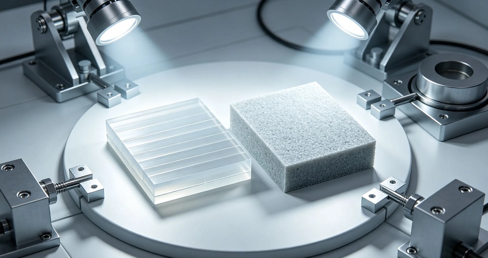
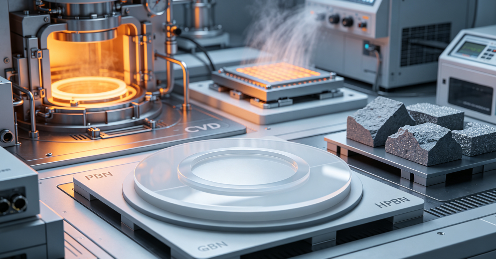
The first decision in manufacturing customized BN components is selecting the appropriate BN grade. Although all BN materials share the same basic chemical composition, different manufacturing routes create significant differences in purity, microstructure, mechanical behavior, and thermal properties. Hot-pressed boron nitride (HPBN) is commonly selected for customized mechanical components because it provides excellent machinability. Its layered crystal structure allows engineers to machine holes, grooves, threads, slots, and complex geometries that are difficult to achieve with harder ceramics such as alumina or silicon carbide. This makes HPBN suitable for prototype development, customized fixtures, insulating rings, and structural components. Pyrolytic boron nitride (PBN), produced through chemical vapor deposition, provides higher purity and a highly oriented layered structure. It is typically selected for applications requiring extremely low contamination, high vacuum compatibility, and direct exposure to semiconductor materials.
| Property | HPBN (Hot-Pressed BN) | PBN (Pyrolytic BN) |
|---|---|---|
| Manufacturing Method | Hot pressing BN powder | Chemical vapor deposition |
| Purity Level | High, grade dependent | Extremely high |
| Machinability | Excellent | Limited compared with HPBN |
| Mechanical Strength | Higher bulk strength | High purity advantage |
| Complex Geometry | Excellent | More difficult |
| Typical Application | Insulators, rings, fixtures, supports | Crucibles, wafer-facing components, high-purity parts |
| Semiconductor Suitability | Suitable for qualified applications | Preferred for contamination-sensitive processes |
In boron nitride semiconductor manufacturing, the correct material choice depends on the position of the component inside the equipment. A wafer-facing component may require PBN because contamination control is the highest priority, while a structural insulation component may benefit more from HPBN because machining flexibility and mechanical stability are more important.
Custom Manufacturing Process of Boron Nitride Components
The manufacturing process begins with engineering drawing review. Unlike metal components, BN ceramics have unique machining characteristics because they are hard but relatively brittle. Engineers must consider wall thickness, corner radius, hole geometry, stress concentration areas, and thermal expansion behavior during the design stage. The first step is material preparation. The selected BN blank must meet requirements for density, purity, and microstructure. For semiconductor applications, material certification and impurity control are especially important because trace contamination can influence wafer quality. The second step is precision machining. One major advantage of HPBN is that it can often be machined using conventional ceramic machining techniques rather than requiring extensive diamond grinding. CNC machining can create complex structures including holes, grooves, stepped surfaces, thin walls, and customized profiles.
During machining, controlling contamination is critical. Cutting fluids containing organic compounds or metallic residues should be avoided for semiconductor-grade applications. After machining, components normally require cleaning procedures to remove particles and surface residues. The final stage includes dimensional inspection, surface evaluation, and packaging. Critical dimensions such as inner diameter, outer diameter, flatness, concentricity, and surface roughness should be verified according to engineering requirements.
Manufacturing Customized BN Insulator Rings, Gas Nozzles, and Wafer Chuck Parts
Custom Boron Nitride Insulator Rings
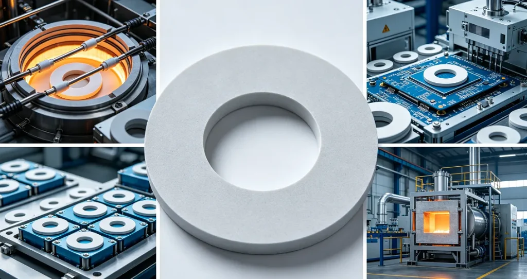
BN insulating rings are widely used where electrical isolation and thermal stability are required simultaneously. Compared with polymer insulation materials, BN rings can maintain performance at temperatures where organic materials fail. Their low dielectric loss, chemical stability, and resistance to thermal shock make them suitable for high-temperature semiconductor and vacuum equipment. During manufacturing, engineers must carefully control ring geometry because uneven thickness or poor flatness can affect assembly precision and thermal distribution. Important parameters include inner and outer diameter tolerance, thickness variation, surface finish, and mechanical strength.
Custom Boron Nitride Gas Nozzles
Gas nozzles used in semiconductor equipment require excellent chemical compatibility and dimensional stability. The nozzle geometry directly influences gas distribution uniformity, which can affect deposition thickness and process repeatability. BN is attractive for nozzle applications because it maintains stability under high temperatures and has low chemical reactivity. However, nozzle manufacturing requires precise internal channels, smooth surfaces, and controlled contamination levels. For example, in plasma processing or deposition equipment, a poorly manufactured nozzle may create uneven gas flow or generate particles that affect wafer yield. Therefore, machining accuracy and surface quality are critical.
Custom Boron Nitride Wafer Chuck Parts
Wafer chuck components require precise thermal management because temperature uniformity directly influences semiconductor processing results. BN is used in certain wafer support and thermal fixture applications because it combines electrical insulation with useful thermal conductivity. The design of wafer chuck parts must consider thermal expansion matching, flatness, mechanical support, and contamination control. Even small dimensional deviations may influence wafer positioning or temperature distribution. In boron nitride semiconductor manufacturing, customized wafer-related ceramic components require cooperation between material engineers and equipment designers to ensure the final part matches the complete process requirement.
Typical Technical Parameters for Customized BN Components
| Parameter | Typical Requirement |
|---|---|
| Material | HPBN / PBN |
| Purity | ≥99% depending on grade |
| Density | 1.9–2.25 g/cm³ |
| Maximum Temperature (Inert/Vacuum) | Up to 2000°C depending on grade |
| Electrical Resistivity | >10¹² Ω·cm |
| Thermal Conductivity | Approximately 20–80 W/m·K depending on orientation |
| Machining Tolerance | Around ±0.05–0.10 mm depending on geometry |
| Surface Finish | Machined, polished, or customized |
Integration of BN Auxiliary Components in Semiconductor and High-Temperature Systems
Besides structural components such as insulating rings, gas nozzles, and wafer chuck parts, boron nitride is also widely used in auxiliary ceramic components that support thermal management, separation, insulation, and process stability. These components may not always directly contact wafers, but their performance can significantly influence the reliability of the entire semiconductor system. A Boron Nitride Firing Plate is commonly used in high-temperature firing, sintering, and thermal processing environments because it provides excellent thermal shock resistance and chemical stability. Compared with conventional ceramic plates, BN firing plates can reduce sticking problems with many materials and maintain stable performance during repeated heating cycles. For semiconductor-related thermal processes, the firing plate must have controlled flatness, low contamination characteristics, and sufficient mechanical strength to maintain dimensional stability during long-term operation.
A Boron Nitride Gasket is designed for applications requiring high-temperature sealing, electrical insulation, or component separation. Unlike metallic sealing materials that may react with certain environments, BN gaskets provide excellent chemical resistance and maintain insulation properties at elevated temperatures. In vacuum and semiconductor equipment, gasket materials must be carefully selected because trapped gases, decomposition products, or surface contamination may affect process stability. Flexible BN materials are also important in customized semiconductor equipment. A Boron Nitride Insulating Paper provides lightweight thermal insulation and electrical isolation where rigid ceramic components are not suitable. It can be used in areas requiring thin protective layers, thermal barriers, or electrical separation. Due to its flexibility and high-temperature capability, BN paper materials provide engineers with additional design freedom when developing compact thermal structures.
Similarly, Boron Nitride Release Paper is often used where clean separation between high-temperature materials is required. Its excellent non-wetting characteristics and chemical stability help reduce adhesion between contacting surfaces during thermal processing. This makes BN release materials valuable in applications where maintaining surface quality and minimizing contamination are important. In boron nitride semiconductor manufacturing, these auxiliary components are selected based on their specific function within the equipment system. The engineering objective is not only to choose a high-temperature material but to create a stable thermal, electrical, and contamination-controlled environment.
Quality Control Requirements for Custom BN Manufacturing
For semiconductor applications, custom manufacturing quality control is as important as material selection. A BN component that meets dimensional requirements but contains uncontrolled contamination may fail during actual operation. The first quality control step is incoming material inspection. Manufacturers should verify material grade, purity, density, and relevant physical properties before machining. For high-purity semiconductor applications, trace element analysis may be required to confirm that metallic impurities remain within acceptable limits.
Dimensional inspection is another critical stage. BN ceramics cannot be adjusted after final installation in the same way as metals, so dimensional accuracy must be achieved during machining. Important inspection items include diameter tolerance, thickness tolerance, flatness, parallelism, concentricity, and surface condition. Surface cleanliness is especially important for vacuum and semiconductor environments. After machining, BN components should undergo appropriate cleaning procedures to remove particles and processing residues. Packaging should also prevent contamination during transportation and storage.
| Quality Control Item | Engineering Purpose |
|---|---|
| Material purity analysis | Confirm contamination control capability |
| Density measurement | Evaluate microstructure stability |
| Dimensional inspection | Ensure assembly compatibility |
| Surface roughness testing | Reduce particle generation |
| Visual inspection | Detect machining defects |
| Thermal testing | Verify high-temperature stability |
| Packaging inspection | Prevent contamination after production |
A professional BN supplier should provide not only the ceramic component but also the technical information required for application qualification.
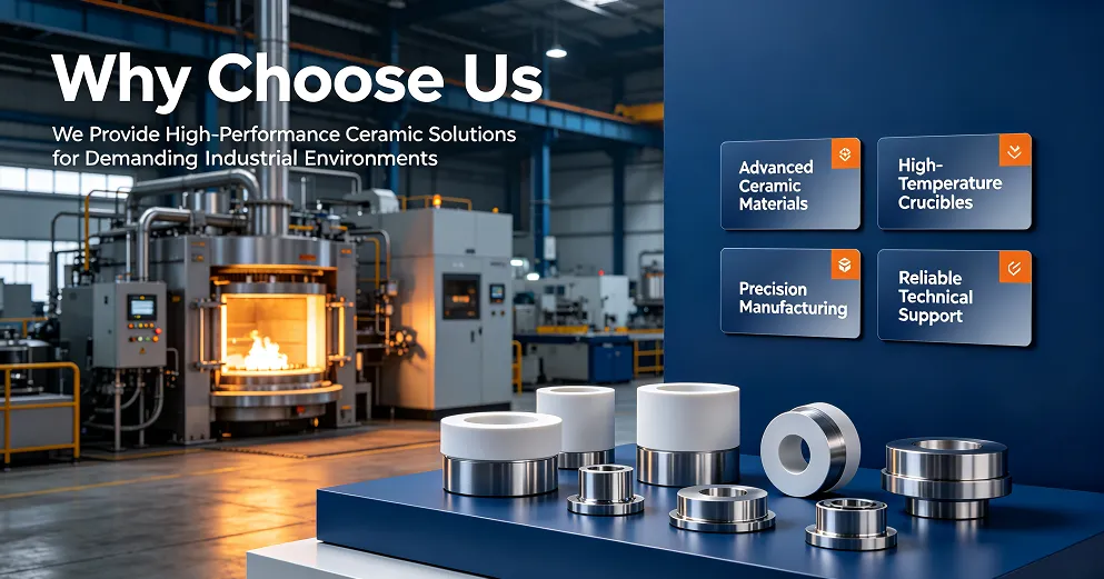
JianXun Technology Company Profile
JianXun Technology Co., Ltd. specializes in the manufacturing and supply of finished advanced ceramic components, including Boron Nitride, Alumina, and Silicon Carbide products for semiconductor equipment, high-temperature processing, thermal management, and electrical insulation applications.
With engineering-focused manufacturing capabilities, JianXun provides customized ceramic solutions according to customer drawings, material requirements, operating conditions, and performance specifications. The company focuses on delivering reliable ceramic components with controlled purity, stable thermal properties, precision dimensions, and excellent chemical resistance.
JianXun supports applications requiring customized BN components such as insulating parts, thermal fixtures, protection components, and semiconductor-related ceramic structures. Through material selection, precision machining, quality inspection, and customized production processes, JianXun aims to provide advanced ceramic solutions for demanding industrial environments.
Payment Terms: T/T, PayPal, Credit Card, Western Union, or other agreed payment methods.
Shipment Terms: Products can be shipped by express, air freight, or sea freight depending on product size, quantity, and customer requirements.
Storage Conditions: Boron nitride ceramic products should be stored in a clean, dry environment and protected from moisture, dust, and chemical contamination before installation.
FAQs
Q1: What information should engineers provide when requesting customized boron nitride components?
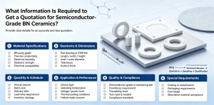
When requesting a customized BN component, engineers should provide more than a simple drawing because the operating environment strongly influences material selection and manufacturing requirements. The most important information includes component dimensions, tolerance requirements, surface finish, operating temperature, atmosphere condition, vacuum level, electrical requirements, thermal cycling conditions, and expected service life. For semiconductor applications, engineers should also specify whether the component is located near the wafer, exposed to process gases, or used only as a supporting structure. A BN component used in a high-temperature furnace insulation system may require different purity and mechanical properties compared with a wafer chuck component inside a semiconductor processing chamber. In boron nitride semiconductor manufacturing, understanding the complete application environment allows manufacturers to select the correct BN grade, machining method, and quality control procedure.
Q2: Can boron nitride components be manufactured according to complex engineering drawings?
Yes. One of the major advantages of hot-pressed BN is its excellent machinability compared with many other advanced ceramics. BN can be processed into complex geometries including rings, plates, nozzles, holes, channels, grooves, thin-wall structures, and customized profiles according to engineering drawings. However, BN machining requires an understanding of ceramic behavior. Although BN is relatively easy to machine compared with alumina or silicon carbide, excessive mechanical stress, unsuitable tooling, or incorrect machining parameters may cause edge chipping or dimensional variation. Therefore, experienced manufacturers evaluate the component design before production and may recommend adjustments to corner radius, wall thickness, or machining sequence to improve reliability. For semiconductor applications, machining accuracy alone is not enough. The final component must also maintain surface cleanliness and low contamination characteristics after processing.
Q3: How do manufacturers prevent contamination during custom BN machining?
Preventing contamination during BN machining requires strict control of the entire manufacturing environment. Unlike ordinary industrial ceramic machining, semiconductor-grade BN components must avoid introducing foreign particles, metallic residues, organic compounds, or machining chemicals that may later affect wafer processing. Manufacturers typically control tooling selection, machining conditions, cleaning procedures, and packaging methods. Dry machining or specially controlled machining processes are often preferred because conventional cutting fluids may leave residues that become contamination sources during high-temperature operation. After machining, components should be cleaned and inspected before shipment. Surface particles, fingerprints, dust, and moisture exposure must be minimized. In boron nitride semiconductor manufacturing, contamination control is a continuous process that begins with raw material selection and continues until final installation inside the equipment.
Q4: What is the difference between standard BN parts and semiconductor-grade customized BN parts?
The main difference is the level of material control and manufacturing requirements. Standard BN components are often designed for general high-temperature, electrical insulation, or mechanical applications where extreme contamination control is not the primary requirement. Semiconductor-grade customized BN components require much stricter control of purity, density, surface quality, and processing history. Semiconductor applications often require detailed information about impurity levels, manufacturing methods, thermal behavior, and vacuum compatibility. Customized BN parts may also require tighter dimensional tolerances because they must integrate precisely with complex semiconductor equipment. Therefore, semiconductor-grade BN manufacturing is not simply producing the same ceramic shape with higher purity. It requires engineering consideration of the entire process environment and long-term reliability requirements.
Q5: Why is boron nitride selected for customized semiconductor ceramic components?
Boron nitride is selected because it provides a unique combination of properties that are difficult to achieve with other ceramics. It offers high-temperature stability, excellent electrical insulation, chemical resistance, thermal shock resistance, and relatively easy machining compared with many hard ceramics. For customized semiconductor components, these properties allow engineers to design parts that can withstand demanding thermal cycles while maintaining electrical and chemical stability. Components such as insulating rings, gas nozzles, wafer supports, thermal plates, and separation structures can benefit from BN’s stable performance. In boron nitride semiconductor manufacturing, the value of BN comes from its ability to provide reliable performance in environments where contamination control, temperature resistance, and dimensional stability are all critical requirements.