Advanced Technical Ceramics, Precision Alumina, Silicon Carbide, Crucible Parts



Is Boron Nitride Machinable to Tight Tolerances for Semiconductor Parts?
When engineers specify ceramic components for semiconductor equipment, “machinable” is not enough. The real question is whether the material can be processed into the required geometry, dimensional tolerance, surface condition, flatness, concentricity, and edge quality without sacrificing the thermal, electrical, chemical, and purity characteristics that make the ceramic useful in the first place. This is particularly important for boron nitride, because its relatively soft, layered crystal structure gives it an unusual combination of high-temperature performance and machinability compared with many conventional technical ceramics. For semiconductor equipment, however, the answer depends strongly on the BN grade and manufacturing route. Hot-pressed h-BN can be machined into rings, plates, sleeves, nozzles, spacers, crucibles, and other complex components using conventional machining processes. PBN, by contrast, is produced by chemical vapor deposition and has a highly oriented layered structure, so its fabrication route and dimensional-control strategy are different. Therefore, asking whether boron nitride semiconductor manufacturing parts can achieve tight tolerances should always lead to a second question: Which BN grade, what geometry, what tolerance, and under what thermal and atmospheric conditions?
Industrial suppliers report that machinable BN can be processed into intricate geometries and narrow tolerances, while published examples show that tolerances around ±0.1 mm or tighter can be achievable depending on the material, geometry, equipment, and inspection requirements. The important engineering point is that a tolerance should not be treated as a generic property of “boron nitride.” It is the result of material grade, billet structure, machining method, part geometry, thermal history, and inspection capability working together.
1. Why Boron Nitride Is Easier to Machine Than Many Technical Ceramics
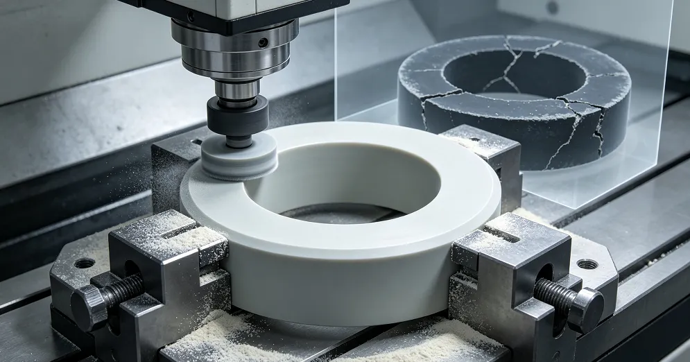
The machinability of BN comes primarily from its hexagonal crystal structure. In h-BN, boron and nitrogen atoms form strongly bonded hexagonal layers, while the bonding between adjacent layers is much weaker. This layered structure produces properties somewhat analogous to graphite: the material has good lubricity and can be mechanically cut, drilled, milled, or otherwise shaped without the extreme machining difficulty associated with dense alumina, silicon carbide, or other highly hard ceramics. This is one reason boron nitride semiconductor manufacturing components can be produced in geometries that would require much more aggressive diamond grinding when manufactured from harder ceramics. Commercial machinable BN grades can be processed using carbide or other conventional tooling depending on the grade, and dry machining is generally preferred because cutting fluids or organic residues can become undesirable contaminants during subsequent high-temperature service.
The machinability should not be interpreted as meaning that BN behaves like aluminum or engineering plastic. BN remains a brittle ceramic. Thin walls, sharp internal corners, small holes, deep grooves, narrow ribs, and unsupported features require careful tool-path design and fixturing. Excessive clamping force can damage the part, while aggressive cutting conditions can generate edge chipping or local delamination. This distinction becomes particularly important in boron nitride semiconductor manufacturing, where dimensional accuracy is only one part of the specification. A component may have to maintain its geometry during repeated heating cycles, remain electrically insulating, avoid introducing metallic contamination, and retain an appropriate surface condition after machining.
2. What “Tight Tolerance” Actually Means for BN Components
There is no single tolerance that can be called “the BN tolerance.” A drawing may contain several different dimensional requirements, and each should be evaluated independently. For example, a semiconductor process ring may require a controlled outside diameter, inside diameter, thickness, flatness, concentricity, and parallelism. A firing plate may have a relatively large overall dimension but a demanding flatness specification. A target-related component may require accurate mounting dimensions while the functional surface has a separate roughness requirement.
The following values are useful as engineering reference points rather than universal guarantees:
| BN Machined Feature | Typical Engineering Consideration | Main Control Factor |
|---|---|---|
| Diameter | Around ±0.05–0.10 mm may be feasible for suitable geometries | CNC turning, tool condition, material grade |
| Thickness | Around ±0.05–0.10 mm depending on size | Grinding / milling process |
| Flatness | Application-specific; large thin plates are more challenging | Residual stress, support, grinding |
| Concentricity | Usually more demanding than simple diameter tolerance | One-setting machining, fixture accuracy |
| Hole diameter | Tight tolerance possible with appropriate tooling | Drill/reaming strategy and edge strength |
| Surface roughness | Depends strongly on process and functional surface | Cutting parameters / finishing |
| Thin-wall geometry | More difficult than bulk geometry | Wall thickness, clamping, vibration |
| Large-area plate | Dimensional tolerance may be achievable while flatness becomes limiting | Billet structure and finishing |
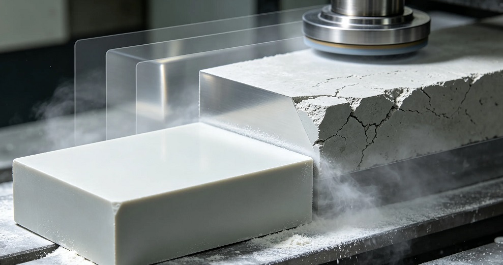
Commercial machining data illustrates why tolerance must be specified according to geometry. Saint-Gobain, for example, publishes different tolerance guidelines for wafers, rods, discs, rings, tubes, crucibles, bars, and plates rather than assigning one universal tolerance to all BN parts. For boron nitride semiconductor manufacturing, this is a much more useful way to evaluate machinability. Instead of asking whether “BN can hold ±0.05 mm,” an engineer should provide the complete drawing and identify which dimensions are functionally critical.
3. Does BN Require Diamond Grinding to Achieve Precision?
Not necessarily. This is one of the advantages of machinable h-BN. Depending on the grade, BN can be machined using carbide tooling, while some composite grades may require more wear-resistant tooling. Grinding can also be used when a finer dimensional or surface finish is required. Published machining guidance for commercial BN grades describes dry machining and identifies different tooling requirements according to grade. For a relatively simple ring or spacer, conventional CNC turning may establish the principal diameter and thickness. For a plate, CNC milling followed by controlled surface finishing may be appropriate. For a component requiring particularly controlled flatness or parallelism, grinding may be introduced as a finishing operation.
The correct process therefore depends on what the drawing actually demands. In boron nitride semiconductor manufacturing, unnecessary grinding can increase cost and processing time, while relying only on rough machining can leave the final dimensional accuracy or surface quality insufficient. A practical manufacturing sequence is often:
BN billet → rough machining → stress-controlled finishing → precision machining → dimensional inspection → cleaning → final packaging
The exact route changes with material grade and geometry, but the principle remains the same: precision comes from process control rather than simply selecting a “precision BN” material.
4. HPBN Machinability vs PBN: A Critical Difference
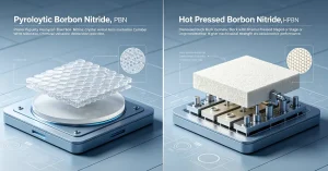
The distinction between HPBN and PBN is particularly important when discussing semiconductor components. Hot-pressed BN, commonly referred to as HPBN, is produced from BN powder through a pressing and high-temperature densification process. The resulting bulk material can be machined into relatively complex shapes and is widely used for insulating and high-temperature structural components. PBN, or pyrolytic boron nitride, is produced through chemical vapor deposition. Instead of starting with a conventional bulk powder compact, gaseous precursors deposit BN onto a substrate and form a highly oriented layered structure. PBN is valued for its very high purity, dense structure, and suitability for contamination-sensitive high-temperature and vacuum applications.
For boron nitride semiconductor manufacturing, the difference is important because a component’s required purity and process environment may be more important than its machining convenience.
| Characteristic | HPBN | PBN |
|---|---|---|
| Manufacturing route | Hot pressing / powder processing | Chemical vapor deposition |
| Structure | Dense h-BN with platelet orientation | Highly oriented layered BN |
| Machinability | Generally very good | More dependent on geometry and fabrication route |
| Complex bulk shapes | Very suitable | More constrained by deposition geometry |
| Purity | Grade dependent | Typically very high |
| Vacuum / contamination-sensitive use | Suitable for qualified grades | Particularly well suited |
| Semiconductor fixtures | Common | Common in demanding applications |
| Crucibles | Suitable for selected processes | Widely used for high-purity applications |
| Thin-wall structures | Possible | Particularly useful for deposited structures |
| Large bulk components | Practical | Limited by deposition/process constraints |
This is why it would be technically incorrect to simply state that PBN is always the “best machinable BN.” PBN is usually selected because of its purity, structure, and process compatibility; HPBN is often selected when a machinable bulk ceramic with larger or more mechanically substantial geometry is required.
5. Why Anisotropy Matters When Machining BN
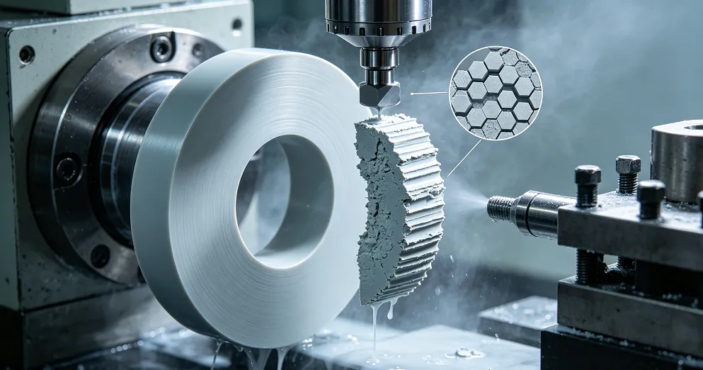
Another issue often overlooked in discussions about boron nitride semiconductor manufacturing is anisotropy. The plate-like BN crystals in hot-pressed material can become preferentially oriented during processing. As a result, thermal conductivity, mechanical behavior, and other physical properties can vary with direction. Saint-Gobain specifically notes that the pressing process produces platelet alignment and recommends considering material orientation when designing and machining parts. This matters in semiconductor equipment because the direction of heat flow may be critical. Imagine a BN ring surrounding a heated region. If thermal conductivity differs substantially between the radial and axial directions, simply rotating the part or changing its machining orientation can influence thermal behavior. Similarly, a thin wall machined across an unfavorable material direction may have different resistance to chipping or mechanical damage. Therefore, an engineering drawing for a critical boron nitride semiconductor manufacturing component should ideally define not only dimensions and tolerances but also material grade and, where relevant, material orientation.
6. Can BN Separation Rings Be Machined to Tight Tolerances?
Yes, and rings are actually a good example of where BN’s machinability becomes valuable. A BN Separation Ring may require controlled inside and outside diameters, uniform thickness, concentricity, and clean edges. The ring may also sit close to a heated wafer, process chamber, or other ceramic component, making dimensional consistency important for assembly and thermal behavior. The machining challenge increases as the ring becomes thinner or the radial wall becomes narrower. A thick ring has considerably more structural rigidity during machining than a thin ring with a large inner diameter. Tool pressure, clamping, vibration, and edge breakout therefore become increasingly important as the geometry becomes more delicate.
For a Boron Nitride Separation Ring, the engineering approach should focus on three things: maintaining concentricity between the ID and OD, controlling thickness variation around the circumference, and protecting the functional edges from chipping.Where the ring is used in boron nitride semiconductor manufacturing, dimensional inspection should ideally include more than simply measuring the OD. ID, wall thickness, parallelism, flatness, and concentricity may all affect final assembly.
7. What About Boron Nitride Firing Plates?
Firing plates present a different machining problem. A BN Firing Plate may have relatively simple geometry, but its large surface area can make flatness and thermal deformation more important than small dimensional tolerances. A plate that is dimensionally correct at room temperature is not necessarily functionally stable during repeated high-temperature cycles. For this reason, the manufacturing process should consider billet uniformity, internal stress, machining sequence, support during finishing, and thermal exposure. Removing material unevenly from one side of a plate can release residual stresses and cause warpage.
In boron nitride semiconductor manufacturing, this becomes particularly important when a plate functions as a thermal-processing fixture or supports sensitive components. Flatness influences contact conditions, spacing, and heat transfer. Surface contamination and roughness can also matter when the plate is repeatedly exposed to high temperatures. A well-designed BN firing plate therefore requires more than a simple CNC operation. The machining strategy should be designed around the final thermal function of the part.
8. Can Boron Nitride Target Material Be Precision Machined?
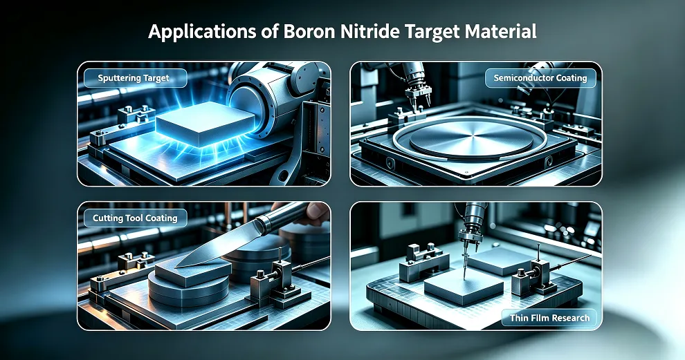
Target-related BN components require a different level of attention because purity, surface condition, and dimensional accuracy may all interact. For BN Target Material, the machining process must avoid introducing contaminants that could compromise the intended process environment. Dry machining is particularly attractive because conventional cutting fluids can leave residues that become problematic during subsequent thermal or vacuum processing. Commercial BN machining guidance specifically recommends avoiding coolants and lubricants for this reason.
At the same time, dimensional precision cannot be considered independently of the target’s final surface. Surface roughness, flatness, edge geometry, mounting dimensions, and cleanliness may all affect how the component performs inside process equipment. For boron nitride semiconductor manufacturing, the correct specification should therefore identify the functional surface separately from non-functional mounting surfaces. Not every surface needs the same tolerance or finish, and treating every dimension as equally critical can unnecessarily increase machining cost.
9. What Machining Problems Are Most Likely to Affect Semiconductor BN Parts?
The most common mistake is assuming that because BN is machinable, every geometry can automatically be manufactured with the same tolerance. The first problem is edge chipping. BN is relatively soft compared with alumina or silicon carbide, but it remains brittle. Small holes, slots, sharp corners, and thin walls can be damaged if the cutting force is too high. The second problem is dimensional instability after machining. Large or thin components can respond differently to stress release, handling, and thermal cycling. This is especially relevant for plates and thin rings. The third problem is material orientation. A hot-pressed BN billet can have direction-dependent properties, so the orientation of the finished component should be considered where thermal or mechanical performance is critical. The fourth problem is contamination. Semiconductor components cannot be treated like ordinary industrial ceramic parts. Cutting fluids, dirty tooling, improper packaging, dust, and handling residues can all become concerns. The fifth problem is over-specification. Requiring ±0.01 mm on every dimension may sound technically impressive, but if the equipment does not need that accuracy, it can increase cost without improving process performance. Good ceramic engineering means identifying functional tolerances rather than applying unnecessarily tight tolerances everywhere.
10. How Should Engineers Specify Tight-Tolerance BN Parts?
For a precision boron nitride semiconductor manufacturing component, the drawing should contain enough information for the manufacturer to evaluate the complete manufacturing problem.
| Specification | Why It Matters |
|---|---|
| BN grade | Determines purity, strength, machinability and thermal behavior |
| Manufacturing route | HPBN, PBN or another BN route changes processing characteristics |
| Material orientation | Important for anisotropic properties |
| Overall dimensions | Defines machining envelope |
| Critical tolerances | Identifies dimensions affecting assembly/function |
| Flatness | Important for plates, wafers and support surfaces |
| Parallelism | Controls contact and alignment |
| Concentricity | Important for rings, tubes and rotating/assembled parts |
| Surface roughness | Influences contact, contamination and process behavior |
| Edge radius/chamfer | Reduces chipping risk |
| Operating temperature | Determines thermal stability requirements |
| Atmosphere | Vacuum, inert gas or air changes service limits |
| Purity requirement | Critical for contamination-sensitive processes |
| Cleaning requirement | Prevents machining residues from entering the process |
| Quantity | Influences tooling and process optimization |
This information allows the manufacturer to decide whether the part should be produced from HPBN billet, PBN material, or another BN grade and whether CNC machining, grinding, or a combination of processes is appropriate.
11. Tight Tolerance Does Not Mean Tight Tolerance Everywhere
One of the most important principles in boron nitride semiconductor manufacturing is functional dimensioning. Consider a BN ring with an OD of 100 mm. The mounting diameter may need a relatively tight tolerance because it interfaces with another component. The external edge, however, may not require the same accuracy. Similarly, a firing plate may require excellent flatness over its functional area while its outer edge can tolerate a larger dimensional deviation. This approach allows the machining process to concentrate its highest precision where it actually affects equipment performance. A technically mature ceramic supplier should therefore review the drawing rather than simply quote a generic “±0.05 mm precision.” Geometry, material grade, wall thickness, machining direction, inspection method, and quantity all influence the achievable result.
12. Recommended BN Selection for Semiconductor Parts
For engineers selecting a material for boron nitride semiconductor manufacturing, the decision can be simplified into three practical routes.
I. Choose HPBN when machinability and bulk geometry are the priority.
HPBN is attractive for rings, spacers, plates, insulating structures, sleeves, nozzles, and other components requiring conventional machining of a bulk ceramic. It is especially useful when the component has relatively substantial dimensions or complex machined features.
II. Choose PBN when purity and process contamination are the primary concerns.
PBN is particularly attractive for demanding vacuum, crystal-growth, MOCVD, MBE, and other high-purity semiconductor-related environments. Its CVD-derived structure and high purity make it suitable for applications where contamination control is more important than straightforward bulk machining.
III. Choose the grade according to the actual process environment.
Temperature, atmosphere, thermal cycling, electrical insulation, contact chemistry, mechanical load, purity, dimensional stability, and required geometry should all be evaluated together. Maximum temperature values should never be considered without specifying the atmosphere because BN behaves very differently in vacuum/inert environments and oxidizing conditions.
13. Practical Comparison: Which BN Route Is Better for Tight-Tolerance Parts?
| Requirement | HPBN | PBN | Engineering Preference |
|---|---|---|---|
| Conventional CNC machining | Excellent | Application dependent | HPBN |
| Complex bulk geometry | Excellent | Limited by fabrication route | HPBN |
| Very high purity | Grade dependent | Excellent | PBN |
| Vacuum semiconductor equipment | Excellent with qualified grade | Excellent | Application dependent |
| MOCVD/CVD components | Suitable | Excellent for high-purity applications | PBN / qualified HPBN |
| Large thick component | Excellent | Less suitable | HPBN |
| Thin-wall deposited structure | Limited by billet geometry | Excellent | PBN |
| Tight dimensional control | Achievable | Achievable through suitable fabrication/finishing | Both |
| Large flat plate | Practical | Geometry dependent | HPBN |
| Contamination-sensitive application | Requires grade/cleaning control | Strong advantage | PBN |
| Machining cost | Generally more practical | Depends strongly on geometry | HPBN |
The table should not be interpreted as saying that one material wins every category. In real boron nitride semiconductor manufacturing, the best solution is determined by the combination of purity, geometry, temperature, atmosphere, and dimensional requirements.
14. How We Approach Precision Boron Nitride Components
For JianXun Technology Co., Ltd., the objective is not simply to supply a BN blank and leave the engineering problem to the customer. Finished ceramic components should be evaluated according to their intended process environment, drawing requirements, material grade, dimensional tolerances, and thermal function. Our product range includes finished Boron Nitride components such as separation rings, firing plates, target-related components, insulating sleeves, nozzles, rods, and other customized ceramic parts. For precision applications, the drawing should define the critical dimensions, tolerances, surface requirements, operating temperature, atmosphere, and purity requirements so that the material and machining route can be evaluated together.
Company Profile
JianXun Technology Co., Ltd. specializes in finished advanced ceramic components for semiconductor, high-temperature, thermal-processing, and electrical-insulation applications. Our product range covers Boron Nitride, Alumina, and Silicon Carbide products, including customized ceramic parts manufactured according to application and drawing requirements.
Payment Terms: T/T, PayPal, Credit Card, Western Union, or other agreed methods.
Shipment Terms: Express, air freight, or sea freight according to product size, quantity, and customer requirements.
Storage Conditions: Store in a clean, dry environment and keep the original protective packaging until use.
FAQs
Q1: Can boron nitride be machined to tight tolerances for semiconductor components?
Yes, machinable boron nitride can be manufactured to relatively tight dimensional tolerances, but the achievable accuracy depends on the BN grade, component geometry, wall thickness, material structure, machining method, and inspection requirements. Hot-pressed h-BN is generally easier to machine than harder technical ceramics such as alumina and silicon carbide because its layered crystal structure and comparatively low hardness allow turning, milling, drilling, and other precision machining operations. However, BN remains a brittle ceramic, so thin walls, small holes, sharp internal corners, deep grooves, and large thin plates require more careful process control. For boron nitride semiconductor manufacturing components, engineers should not evaluate tolerance as a single ± value; dimensional tolerance, flatness, parallelism, concentricity, surface roughness, and edge condition should be considered according to the actual assembly and thermal function of the component.
Q2: What factors determine the dimensional accuracy of a machined boron nitride part?
The final tolerance of a BN component is determined by much more than the CNC machine itself. Material grade and internal structure influence how the part responds to cutting forces, while geometry determines the rigidity of the workpiece during machining. For example, a thick BN ring can generally be machined more easily than a thin-wall ring with a large internal diameter, while a large firing plate may have relatively simple dimensions but require significantly tighter control of flatness and warpage. Machining sequence is also important because removing material from different surfaces can release internal stresses and produce dimensional changes during finishing. In boron nitride semiconductor manufacturing, engineers should therefore specify critical dimensions together with flatness, concentricity, parallelism, surface roughness, chamfer or edge requirements, and the operating temperature. This allows the manufacturer to determine whether conventional machining, precision milling, turning, grinding, or a combined finishing process is appropriate.
Q3: Is HPBN or PBN better for precision semiconductor components?
The choice between HPBN and PBN should be based on the function of the component rather than simply asking which material is more precise. HPBN is a bulk hot-pressed BN ceramic and is generally advantageous when the component requires conventional machining, relatively complex three-dimensional geometry, larger dimensions, or substantial mechanical support. PBN is produced by chemical vapor deposition and has a highly oriented layered structure, very high purity, and a dense surface, making it particularly attractive for contamination-sensitive vacuum, crystal-growth, MOCVD, and other high-temperature semiconductor processes. In boron nitride semiconductor manufacturing, PBN is often selected when purity, low contamination, and process compatibility dominate the specification, while HPBN can be the more practical choice when machinability and bulk geometry are the primary requirements. Therefore, a tight dimensional tolerance alone is not sufficient to determine the appropriate BN grade.
Q4: How should engineers control machining quality for BN rings, firing plates, and target components?
For semiconductor-grade BN components, machining quality should be controlled as part of the complete manufacturing process rather than treating dimensional machining as an isolated operation. A Boron Nitride Separation Ring, for example, may require controlled inner and outer diameters, concentricity, uniform wall thickness, parallelism, and clean edges because dimensional errors can influence alignment and assembly. A Boron Nitride Firing Plate may place greater emphasis on flatness, thickness uniformity, surface condition, and resistance to deformation during repeated thermal cycles. For Boron Nitride Target Material, surface condition, mounting dimensions, cleanliness, and contamination control can become equally important because residues introduced during machining may affect subsequent high-temperature or vacuum processing. The machining route should therefore be selected according to the functional surfaces and critical dimensions shown on the engineering drawing, rather than applying the same tolerance and finishing method to every feature.
Q5: What should be specified when ordering tight-tolerance boron nitride semiconductor parts?
An engineering drawing is the most reliable starting point because the required tolerance must be evaluated together with the operating environment and material grade. The specification should identify the BN grade or required material characteristics, overall dimensions, critical dimensional tolerances, flatness, parallelism, concentricity where applicable, surface roughness, edge treatment, operating temperature, atmosphere, purity requirements, and quantity. For components used in boron nitride semiconductor manufacturing, it is also important to distinguish functional dimensions from non-critical dimensions; imposing extremely tight tolerances on every feature can increase machining cost without improving process performance. The manufacturer should also evaluate whether the part is better produced from HPBN, PBN, or another BN grade, and whether CNC machining, grinding, or multiple finishing operations are required. This engineering-based specification approach provides a more realistic route to consistent precision than simply requesting a “high-precision boron nitride component.”