Advanced Technical Ceramics, Precision Alumina, Silicon Carbide, Crucible Parts



What Binders or Impurities in Boron Nitride Ceramic Can Contaminate Silicon Wafers?
Why Contamination Control Matters for Boron Nitride Used in Semiconductor Equipment
In semiconductor manufacturing, every material placed near a silicon wafer must be evaluated not only for thermal stability and mechanical performance but also for its contamination potential. Advanced ceramics such as boron nitride (BN) are widely used in high-temperature semiconductor equipment because of their excellent electrical insulation, chemical stability, thermal shock resistance, and ability to maintain performance under extreme processing conditions. However, not all BN ceramics have the same purity level or contamination behavior. The manufacturing route, binder system, raw material quality, residual impurities, and surface treatment process can significantly influence whether a BN component is suitable for sensitive wafer processing environments. For semiconductor engineers, the key question is not simply whether BN is a high-performance ceramic. The more important question is whether the specific BN grade can maintain a clean process environment without introducing unwanted elements into the wafer surface or thin-film structure. In boron nitride semiconductor manufacturing, contamination control is a fundamental design requirement because even trace levels of metallic elements, boron-containing compounds, carbon residues, or binder-derived species may influence electrical properties, crystal quality, deposition uniformity, and device reliability.
Boron nitride itself is chemically stable and is often selected precisely because it produces fewer contamination concerns compared with many alternative materials. However, conventional sintered BN ceramics may contain additives or binders used to improve densification and mechanical properties. These additional phases can become potential contamination sources under high temperature, vacuum, plasma, or reactive gas environments. Therefore, engineers must understand not only the BN crystal structure but also the complete manufacturing history of the ceramic component. Studies investigating BN used in silicon-related high-temperature processes have shown that certain binder-containing BN grades may release volatile boron-, nitrogen-, calcium-, or oxygen-containing species under specific conditions. These released species can interact with silicon materials and affect quality. This does not mean all BN ceramics are unsuitable for semiconductor applications; rather, it highlights why semiconductor-grade BN requires strict control of composition and processing.
How Binders Influence the Purity of BN Ceramic
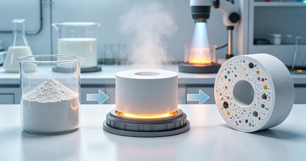
Traditional hot-pressed BN ceramics often require some form of densification assistance because pure hexagonal BN powder has a layered structure and is difficult to sinter through conventional methods. Without appropriate processing, the material may retain excessive porosity and insufficient mechanical strength. Historically, different oxide-based additives or binder systems have been used to improve densification. Typical binder-related components may include calcium borates, boron oxide-related phases, silicon-containing compounds, aluminum-containing compounds, or other sintering aids depending on the manufacturing technology. These materials can improve density and mechanical properties, but they may introduce additional chemical species that are undesirable in ultra-clean semiconductor environments.
For example, calcium-containing binders can become a concern because calcium is a metallic impurity that may affect silicon quality. Some studies have reported that BN grades containing calcium borate binders can generate volatile species during high-temperature reactions, creating potential contamination pathways. In boron nitride semiconductor manufacturing, engineers usually distinguish between general industrial BN ceramics and semiconductor-grade BN ceramics. General industrial grades may prioritize mechanical strength, machinability, or cost efficiency, while semiconductor-grade materials prioritize purity, low outgassing, and controlled impurity levels.
The influence of binders can be summarized as follows:
| Binder / Residual Component | Possible Source | Potential Semiconductor Concern | Engineering Control Method |
|---|---|---|---|
| Calcium borate | Hot pressing additives | Calcium contamination, volatile species release | Use high-purity binder-free or controlled BN grades |
| Boron oxide (B₂O₃) | Oxidized BN phases or sintering additives | Boron diffusion or surface reaction | Control oxygen exposure and material purity |
| Silicon-containing phases | Processing additives or contamination | Silicon-related impurity variation | Trace element analysis |
| Aluminum compounds | Raw materials or additives | Metallic contamination risk | High-purity powder selection |
| Carbon residues | Organic processing or graphite contact | Carbon contamination during heating | Controlled machining and cleaning |
The important point is that binders are not automatically harmful. In many industrial applications, controlled additives can improve ceramic performance. The issue is whether those additives are compatible with the semiconductor process environment.
Main Impurities That Can Affect Silicon Wafer Quality
The contamination sensitivity of semiconductor processes is extremely high because silicon devices rely on precisely controlled electrical properties. Certain impurities that appear insignificant in conventional ceramics can become critical when introduced into semiconductor materials. Metallic impurities are among the most concerning. Elements such as iron, copper, sodium, potassium, calcium, magnesium, and aluminum can diffuse into silicon or interact with oxide layers. These impurities may create defect states, reduce carrier lifetime, increase leakage current, or affect device reliability. Boron is another special case because it is intentionally used as a dopant in silicon technology. However, uncontrolled boron contamination is different from controlled doping. Excess boron release from BN components can change local concentration profiles and negatively affect process precision.
| Impurity Type | Possible Origin in BN Ceramic | Effect on Silicon Wafer |
|---|---|---|
| Calcium (Ca) | Binder residues | Metallic contamination and quality degradation |
| Iron (Fe) | Raw material impurities | Deep-level defects in silicon |
| Copper (Cu) | Processing contamination | Electrical reliability problems |
| Sodium (Na) | Raw materials or handling | Mobile ion contamination |
| Boron (B) | BN decomposition or oxide phases | Uncontrolled doping effects |
| Carbon (C) | Organic residues or graphite contact | Defect formation and process variation |
| Oxygen-related species | Surface oxidation or moisture | Chemical interaction during heating |
Trace analysis methods such as ICP-based techniques are commonly used to identify impurity levels in BN materials. Research has demonstrated the ability to measure elements including Al, Ca, Cr, Fe, Mg, Mo, Na, Si, Ti, and V in BN samples for quality control purposes. For engineers working with boron nitride semiconductor manufacturing, impurity analysis should be considered part of material qualification rather than an optional inspection step.
PBN vs HPBN: Different Contamination Risks
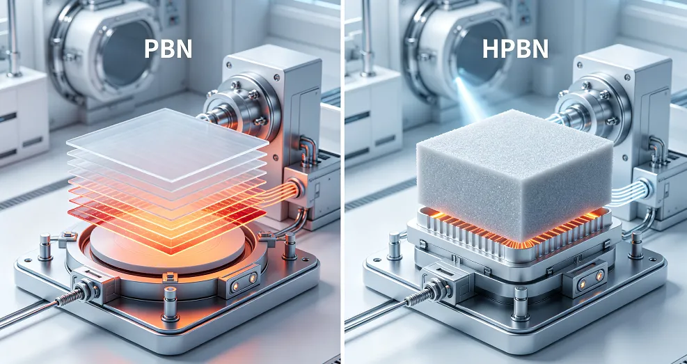
The manufacturing method has a significant influence on contamination behavior. Two major BN categories used in semiconductor-related applications are pyrolytic boron nitride (PBN) and hot-pressed boron nitride (HPBN). PBN is produced through chemical vapor deposition. Because the material is deposited directly from gaseous precursors, the manufacturing process can achieve extremely high purity and a dense layered structure. It does not require conventional sintering binders, which greatly reduces the risk of additive-related contamination. HPBN is produced by hot pressing BN powder. Its advantages include excellent machinability, larger component availability, and easier production of complex shapes. However, engineers must carefully evaluate the specific grade because different HPBN products may use different densification approaches.
| Property | PBN | High-Purity HPBN |
|---|---|---|
| Manufacturing Method | Chemical vapor deposition | Hot pressing |
| Binder Requirement | Normally none | Depends on grade |
| Purity Level | Extremely high | Grade dependent |
| Outgassing Performance | Excellent | Very good with controlled processing |
| Complex Machining | Limited | Excellent |
| Typical Semiconductor Use | Crucibles, high-purity process parts | Fixtures, insulation, structural components |
In boron nitride semiconductor manufacturing, selecting between PBN and HPBN depends on the process location and contamination sensitivity. Components directly exposed to wafers, epitaxial materials, or high-temperature reaction zones generally require stricter purity control.
Contamination Control Strategies for BN Components in Semiconductor Equipment
Achieving semiconductor-grade cleanliness requires controlling contamination throughout the entire lifecycle of a BN component, including material selection, manufacturing, machining, cleaning, transportation, and installation. A high-purity BN material can still become a contamination source if improper machining tools, storage conditions, or handling procedures introduce foreign substances onto the surface. The first step is selecting the correct BN grade according to the process environment. Components located close to silicon wafers or semiconductor source materials require stricter purity requirements compared with components used only for mechanical support or external thermal insulation. Engineers should evaluate the component position, operating temperature, vacuum level, atmosphere composition, and expected service lifetime before selecting the material.
Surface preparation is another critical factor. During machining, conventional lubricants, cutting fluids, or contaminated tools may introduce carbon, metallic particles, or organic residues. These contaminants may remain trapped in surface defects and later release during high-temperature operation. Therefore, semiconductor-grade BN components are often machined using controlled processes followed by cleaning procedures designed to minimize contamination. Thermal conditioning is also commonly used before installation. Heating the BN component under vacuum or inert atmosphere can remove physically absorbed moisture and residual gases. This step is especially important for components that operate in ultra-high vacuum environments because even small amounts of released gas can affect chamber stability.
For boron nitride semiconductor manufacturing, contamination control is not only a material issue but also a system-level engineering consideration. The ceramic component, heating system, chamber environment, and process materials must be evaluated together to ensure stable semiconductor production.
How BN Components Are Applied in Semiconductor Equipment
Different BN components perform different functions inside semiconductor systems, and each application has different contamination requirements. A Boron Nitride Nozzle is often used in high-temperature processing environments where controlled gas flow, chemical stability, and thermal resistance are required. In applications involving reactive gases or elevated temperatures, the nozzle material must maintain purity because any released impurity can enter the process stream and affect wafer quality. A Boron Nitride Rod can serve as a structural, insulating, or support component in high-temperature equipment. The main engineering considerations include dimensional stability, electrical insulation, thermal cycling resistance, and contamination control. When used near sensitive semiconductor processes, the rod material must have controlled impurity levels and stable surface characteristics. A Boron Nitride Separation Ring is typically used where clean separation between high-temperature components is required. The ring must prevent unwanted contact between materials while maintaining thermal stability and chemical compatibility. Because separation components may directly influence heat distribution and material interaction, the purity and surface condition of BN are important factors.
For high-temperature sputtering and deposition systems, Boron Nitride Target Material applications require especially strict control because contamination introduced during target operation can directly affect deposited thin films. The target material must maintain stable composition and avoid releasing unwanted particles or impurities during processing. These applications demonstrate that BN selection should be based on the complete engineering function of the component rather than only the ceramic material itself.
Why Binder-Free or High-Purity BN Is Preferred for Critical Semiconductor Processes
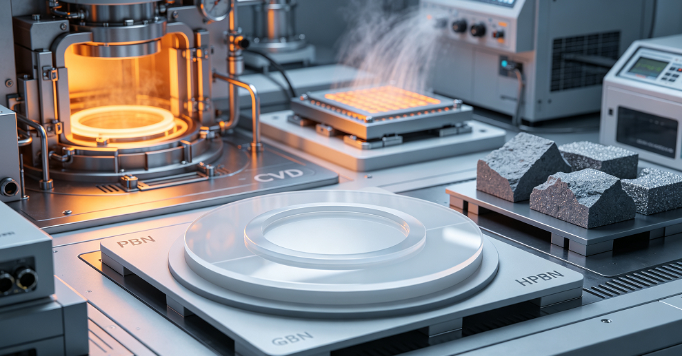
For the most contamination-sensitive semiconductor applications, engineers often prefer BN materials manufactured without conventional binders or with extremely controlled impurity levels. The objective is not simply achieving the highest purity number but reducing unpredictable chemical behavior during operation. Binder-free PBN is widely used in applications where contamination tolerance is extremely low because the material structure is formed directly through deposition. The absence of traditional sintering additives reduces potential sources of metallic contamination. However, this does not mean HPBN should be avoided. High-purity HPBN can provide excellent performance when the manufacturing process is carefully controlled. In many semiconductor equipment designs, HPBN offers advantages because it can be machined into complex geometries that are difficult to produce with PBN.
The engineering decision should therefore balance purity requirements with mechanical and manufacturing requirements.
| Application Requirement | Recommended BN Consideration |
|---|---|
| Direct wafer exposure | Highest purity BN, often PBN |
| High-temperature insulation | High-purity HPBN or PBN depending on environment |
| Complex machined geometry | HPBN advantage |
| Ultra-high vacuum application | Low-outgassing BN grade |
| Thermal separation | BN with controlled thermal properties |
| Long service lifetime | Dense structure with stable impurity control |
In boron nitride semiconductor manufacturing, the best material choice is usually the one that provides the required contamination control while maintaining reliable mechanical and thermal performance.
JianXun Technology Company Profile
JianXun Technology Co., Ltd. specializes in finished advanced ceramic products for semiconductor, high-temperature processing, thermal management, and electrical insulation applications. The company provides customized Boron Nitride, Alumina, and Silicon Carbide ceramic components designed according to engineering drawings, application requirements, and operating conditions.
JianXun focuses on delivering reliable ceramic solutions with controlled purity, thermal stability, electrical insulation performance, chemical resistance, and precision manufacturing capability. The company supports customers requiring advanced ceramic components for demanding industrial environments where material reliability and process stability are critical.
Payment Terms: T/T, PayPal, Credit Card, Western Union, or other agreed payment methods.
Shipment Terms: Products can be shipped by express, air freight, or sea freight according to component size, order quantity, and customer requirements.
Storage Conditions: BN ceramic components should be stored in clean, dry conditions with protective packaging maintained until installation. Avoid exposure to dust, moisture, chemicals, or uncontrolled environments that may affect surface purity.
FAQs
Q1: Can boron nitride ceramic itself contaminate silicon wafers?
Yes, boron nitride ceramic can potentially become a contamination source under certain operating conditions, although high-purity semiconductor-grade BN is specifically developed to minimize this risk. The key point is that contamination does not usually come from the BN crystal structure itself, because hexagonal boron nitride is chemically stable and widely recognized for its excellent high-temperature performance and electrical insulation capability. Instead, contamination concerns are mainly related to residual impurities, manufacturing additives, binder phases, trapped gases, surface residues, and improper processing conditions. During semiconductor manufacturing, BN components may experience high temperatures, vacuum environments, plasma exposure, or reactive gases, which can accelerate the release or migration of trace elements if the material quality is not properly controlled.
For example, conventional industrial BN ceramics may contain sintering aids or residual elements introduced during densification. These additives can improve mechanical strength or reduce porosity, but some metallic elements may become undesirable in wafer processing environments. Even extremely small concentrations of elements such as calcium, iron, sodium, potassium, copper, or aluminum can influence silicon electrical characteristics because semiconductor devices rely on precisely controlled impurity levels. In boron nitride semiconductor manufacturing, engineers therefore need to evaluate not only the nominal purity percentage of BN but also detailed impurity analysis, manufacturing method, density, porosity, surface treatment, and vacuum outgassing performance before selecting a component for wafer-facing applications. The contamination risk also depends strongly on where the BN component is installed inside the equipment. A BN part directly exposed to silicon wafers, epitaxial layers, or deposition materials requires much stricter purity control compared with a structural insulation component located farther away from the process zone. For this reason, semiconductor-grade BN selection is an engineering decision involving the entire process environment rather than simply choosing a ceramic material with high temperature resistance.
Q2: Which impurities in BN are most harmful to silicon wafer processing?
The most concerning impurities in BN ceramics for silicon wafer processing are usually metallic elements, oxygen-related compounds, carbon residues, and uncontrolled boron-containing species. Semiconductor manufacturing is extremely sensitive to trace contamination because silicon devices depend on carefully controlled electrical properties, carrier concentration, and defect levels. Elements that may appear insignificant in conventional industrial ceramics can create serious problems when introduced into semiconductor materials. Metallic impurities such as iron (Fe), copper (Cu), sodium (Na), potassium (K), calcium (Ca), and aluminum (Al) are among the most critical concerns. Iron and copper, for example, can introduce deep-level defects in silicon and negatively affect carrier lifetime, leakage characteristics, and device reliability. Sodium and potassium are mobile ions that may migrate through oxide layers and influence electrical performance. Calcium is particularly important when evaluating certain BN grades because some hot-pressed BN materials may use calcium-containing additives during densification. Under high-temperature conditions, these residual phases may become a potential contamination pathway.
Boron contamination requires special attention because boron is intentionally used as a dopant in semiconductor manufacturing. Controlled boron doping is essential for creating desired electrical properties, but uncontrolled boron release from ceramic components can disturb local concentration profiles and reduce process precision. Carbon contamination is another concern because it may originate from machining residues, organic materials, or improper handling procedures. In high-temperature vacuum environments, these residues can decompose and release carbon-containing species. In boron nitride semiconductor manufacturing, engineers usually evaluate impurities according to the actual application rather than applying one universal standard. A BN crucible, target component, or wafer support located directly inside the process chamber may require extremely low impurity levels, while a thermal insulation component outside the reaction zone may tolerate a different specification. Therefore, understanding the contamination mechanism is more important than simply comparing total purity values.
Q3: Are binders always harmful in hot-pressed boron nitride?
No, binders or sintering additives are not automatically harmful in hot-pressed boron nitride (HPBN). In fact, carefully controlled additives can play an important role in improving the density, mechanical strength, and manufacturing reliability of BN ceramics. Pure hexagonal boron nitride has a layered crystal structure similar to graphite, which provides excellent lubricity and machinability but also makes conventional densification more difficult. Without proper processing assistance, BN may contain excessive porosity, which can reduce mechanical performance and increase gas adsorption. The engineering concern is not whether a BN ceramic contains additives, but whether those additives are compatible with the semiconductor process environment. Some industrial BN grades use sintering aids to achieve higher density and strength, but these additives may introduce elements that are undesirable for advanced semiconductor applications. For example, calcium-based or oxide-based additives may improve densification but require careful evaluation because residual phases could contribute to metallic contamination or outgassing during high-temperature operation.
Modern high-purity HPBN materials are designed with much stricter control over raw materials, additive selection, processing atmosphere, and impurity levels. Many semiconductor applications successfully use HPBN components because they provide excellent machinability, dimensional flexibility, and stable thermal performance. The key is selecting a grade specifically qualified for semiconductor environments rather than using general industrial BN. For boron nitride semiconductor manufacturing, engineers should evaluate HPBN based on measurable performance indicators, including trace-element analysis, density, porosity, thermal stability, vacuum compatibility, and cleaning requirements. A well-controlled HPBN material can provide reliable performance, while an unsuitable grade may introduce contamination risks regardless of its apparent mechanical advantages.
Q4: How can engineers verify whether a BN component is suitable for semiconductor use?
Engineers should verify semiconductor suitability through a combination of material analysis, manufacturing information, and application-specific testing. A purity label alone is not sufficient because two BN materials with similar stated purity levels may have completely different contamination behavior depending on their manufacturing processes, microstructure, and surface condition. The first step is reviewing material characterization data. Important information includes total purity, metallic impurity concentration, density, porosity, manufacturing method, and thermal performance. For semiconductor applications, trace-element analysis is particularly important because elements such as Fe, Cu, Na, K, Ca, and Al can influence silicon device performance even at very low concentrations. Engineers should also consider whether the BN was manufactured through PBN deposition or HPBN processing because the two methods create different microstructures and contamination profiles.
The second step is evaluating the component manufacturing process. Machining, grinding, cleaning, and packaging can significantly influence final component quality. A high-purity BN blank can become unsuitable if machining introduces metallic particles, lubricants, or organic residues. Semiconductor-grade BN components often require controlled machining conditions, specialized cleaning procedures, and contamination-protected packaging. The final evaluation should consider the actual operating environment. Temperature, vacuum level, process gases, thermal cycling frequency, and component location all influence performance. A BN material suitable for a furnace insulation part may not meet the requirements of a wafer-facing component. In boron nitride semiconductor manufacturing, engineers should therefore establish qualification criteria based on the complete process environment instead of selecting materials only from catalog specifications.
Q5: How do BN products such as nozzles, rods, and separation rings avoid contaminating semiconductor processes?
BN components such as nozzles, rods, and separation rings avoid contaminating semiconductor processes primarily through proper material selection, controlled manufacturing, and application-specific design. Although these components may not always directly contact silicon wafers, they can still influence the process environment because they operate near high temperatures, vacuum systems, reactive gases, or sensitive semiconductor materials. A Boron Nitride Nozzle requires excellent chemical stability because it may be exposed directly to process gases or high-temperature reaction zones. Any impurity released from the nozzle surface could potentially enter the gas stream and affect deposition quality. Therefore, nozzle applications usually require high-purity BN with stable composition, low particle generation, and good thermal shock resistance.
A Boron Nitride Rod is often used as a support, insulation, or structural component in high-temperature equipment. Although its function may appear simple, the rod material must maintain dimensional stability and electrical insulation performance during repeated heating cycles. When installed near sensitive process areas, low impurity levels and controlled surface quality become important factors in preventing contamination. A Boron Nitride Separation Ring plays an important role in maintaining clean separation between high-temperature components. It prevents direct contact between materials while maintaining thermal stability and chemical compatibility. Because separation rings often operate at interfaces where materials expand and contract during heating cycles, both purity and mechanical reliability are essential.
For all these BN components, contamination prevention is not achieved by the material alone. It requires a complete engineering approach involving high-quality raw materials, controlled manufacturing, precision machining, proper cleaning, and contamination-free handling. In boron nitride semiconductor manufacturing, every component inside the process environment must be considered as part of the overall contamination-control system.
RELATED POSTS
What Is the Difference Between Pyrolytic Boron Nitride (PBN) and Hot Pressed Boron Nitride (HPBN) in Chip Fabrication?
How to Ensure Low Outgassing and High Purity in Semiconductor-Grade Boron Nitride?