Advanced Technical Ceramics, Precision Alumina, Silicon Carbide, Crucible Parts



What Properties Make Boron Nitride Suitable for Semiconductor Manufacturing?
1. Introduction
In boron nitride semiconductor manufacturing, ceramic materials are exposed to a combination of high temperature, thermal cycling, vacuum, reactive gases, electrical fields, and extremely strict contamination requirements. Under these conditions, material selection cannot be based on a single property such as maximum temperature or hardness. A component may need to conduct heat efficiently while remaining electrically insulating, maintain dimensional stability during repeated thermal cycles, resist chemical attack, generate minimal particles or volatile species, and retain its mechanical integrity after long-term operation. Hexagonal boron nitride (h-BN) is one of the few advanced ceramic materials that can provide this combination of characteristics, which explains its continued use and development in high-temperature semiconductor and electronic-material processing. In boron nitride semiconductor manufaturing, the engineering value of BN comes from the interaction between its crystal structure, thermal properties, dielectric behavior, chemical stability, purity, and machinability rather than from any single specification.
The most commonly used form for high-temperature ceramic components is hexagonal boron nitride. Its layered crystal structure produces strong in-plane bonding and weaker interlayer interaction, resulting in pronounced anisotropy in thermal conductivity, thermal expansion, mechanical behavior, and other physical properties. Depending on purity, density, orientation, porosity, grain structure, and manufacturing process, commercial BN ceramics can show substantially different performance even when they are all described simply as “boron nitride.” Therefore, an engineer selecting BN for semiconductor equipment should evaluate the complete material specification and actual process environment rather than relying on a generic catalog value.
2. Crystal Structure and Its Influence on Semiconductor Applications
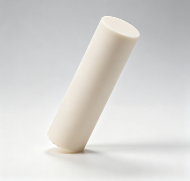
The fundamental properties of boron nitride semiconductor manufaturing materials are closely related to the crystal structure of h-BN. Boron and nitrogen atoms form hexagonal atomic layers through strong covalent bonding, while adjacent layers are connected through relatively weak van der Waals forces. This structure gives h-BN a combination of high thermal conductivity along the basal plane, low friction, good machinability, electrical insulation, and direction-dependent thermal expansion. From an engineering perspective, the layered structure is particularly important because it determines how heat and stress move through a finished component.
For example, if a BN plate is designed to spread heat laterally, its high in-plane thermal conductivity can be advantageous. However, if the same material is used as a through-thickness heat-transfer component, its lower cross-plane conductivity must be considered. This is why a single thermal-conductivity value is often insufficient for semiconductor equipment design. The actual heat-flow direction, material orientation, density, porosity, and operating temperature should all be incorporated into the thermal model. In precision equipment, this directional behavior can influence wafer temperature uniformity, local thermal gradients, thermal stress, and ultimately process stability.
3. High Thermal Conductivity Combined with Electrical Insulation
One of the most important reasons engineers consider BN for semiconductor applications is its unusual combination of thermal conductivity and electrical insulation. Conventional metals provide excellent thermal transport but can create unwanted electrical conduction paths, while many electrical insulating ceramics have relatively low thermal conductivity. High-quality h-BN can bridge this gap by providing efficient heat transfer while maintaining strong electrical insulation.
Depending on the grade, orientation, density, and test conditions, high-performance BN materials can exhibit thermal conductivity from approximately 140 W/(m·K) to more than 400 W/(m·K), with highly oriented h-BN showing considerably higher conductivity along the basal plane. Literature values for high-quality h-BN can reach several hundred W/(m·K), while commercial machinable BN ceramics may have lower effective values because of porosity, grain boundaries, additives, and microstructural differences. Electrical resistivity for high-purity insulating BN grades can commonly exceed 10¹³ Ω·cm. This makes BN particularly useful where a component must transfer or redistribute heat without electrically connecting neighboring structures.
| Property | Representative BN Engineering Range | Engineering Significance |
|---|---|---|
| Density | 1.8–2.2 g/cm³ | Low component mass |
| Thermal conductivity | 140–400+ W/(m·K) | Heat spreading and thermal management |
| Electrical resistivity | >10¹³ Ω·cm | Electrical insulation |
| BN purity | ≥99.9% for selected grades | Contamination control |
| CTE | Approx. −1.5–3.8 × 10⁻⁶ K⁻¹, orientation dependent | Dimensional stability |
| Dielectric band gap | Approx. 5–6 eV | High electrical insulation |
| Maximum temperature | Application and atmosphere dependent | High-temperature processing |
| Machinability | Good for selected BN grades | Complex ceramic geometries |
These values are engineering reference ranges rather than universal specifications. The actual performance of a finished component must be confirmed according to the supplier’s grade, test method, crystallographic orientation, temperature, density, and geometry.
4. Excellent Dielectric Properties
Electrical insulation is another major reason for the increasing interest in boron nitride semiconductor manufaturing. Hexagonal BN has a wide band gap commonly reported around 5–6 eV, making it a strong electrical insulator. At the same time, its thermal conductivity can be substantially higher than that of many conventional insulating ceramics. This combination is valuable when semiconductor equipment requires electrical isolation without completely blocking heat transfer. In high-temperature processing systems, BN can be used for insulating supports, spacers, rings, fixtures, and other components positioned near electrically active structures. Depending on the equipment configuration, these components may need to withstand elevated temperatures while preventing unintended current paths. BN can provide this electrical isolation while maintaining relatively low density and useful thermal transport.
The dielectric performance of BN is also relevant to advanced electronic materials. Thin h-BN is being investigated as a dielectric and insulating layer for two-dimensional electronic structures because of its wide band gap, atomically smooth surfaces, chemical stability, and high dielectric strength. However, engineers should distinguish between thin-film h-BN and bulk machinable BN ceramics. Their grain structure, defect concentration, interfaces, thickness, and processing history are very different, so thin-film electrical data should not automatically be used to specify bulk ceramic components.
The Charm of Boron Nitride Ceramics
5. Low Thermal Expansion and Dimensional Stability
Temperature changes are unavoidable in semiconductor processing, and dimensional stability becomes increasingly important as component tolerances become tighter. A BN component can experience repeated heating and cooling during equipment startup, process operation, recipe changes, and maintenance. If its coefficient of thermal expansion is significantly different from neighboring materials, thermal stress can develop at interfaces and contact points.
Hexagonal BN has a relatively low and strongly anisotropic coefficient of thermal expansion. Representative literature values can range approximately from −1.5 × 10⁻⁶ K⁻¹ to 3.8 × 10⁻⁶ K⁻¹ depending on crystallographic direction, temperature, and material structure. This relatively low expansion can help reduce dimensional changes during temperature excursions. However, engineers should never treat CTE as a single isotropic number when designing precision BN components.
For example, if a BN fixture is assembled with alumina, aluminum nitride, quartz, silicon, graphite, or metal components, the thermal expansion mismatch between the materials should be evaluated across the actual operating temperature range. A component that appears dimensionally stable by itself may still experience significant interface stress if its neighboring material expands at a very different rate. Therefore, CTE matching should be part of the overall mechanical and thermal design rather than a secondary consideration.
6. High-Temperature Stability
High-temperature performance is one of the most recognized advantages of BN ceramics. In vacuum and inert atmospheres, high-purity h-BN can remain stable at temperatures well above 1000 °C, and certain BN materials can operate at temperatures approaching approximately 2800 °C under suitable inert conditions. This makes BN attractive for high-temperature semiconductor processing, crystal growth, thermal treatment, and other processes where conventional polymers, metals, or lower-temperature ceramics may become unsuitable.
However, an important engineering distinction must be made between high-temperature stability and universal oxidation resistance. BN behaves very differently in an inert or vacuum environment compared with an oxygen-containing atmosphere. At elevated temperatures, oxidation can progressively modify the BN surface and influence its mechanical and dimensional behavior. Therefore, stating that “BN can withstand 2800 °C” without identifying the atmosphere can be misleading.
A proper boron nitride semiconductor manufaturing specification should therefore define temperature together with atmospheric conditions. Parameters such as vacuum level, argon or nitrogen flow, oxygen concentration, heating rate, holding time, cooling rate, and number of thermal cycles can all influence the practical lifetime of a BN component.
7. Chemical Stability and Process Compatibility
Semiconductor processing often involves chemically active environments. Depending on the process, ceramic components can be exposed to gases, plasma species, precursor chemicals, cleaning processes, and high-temperature reactions. If the material reacts with the process environment, the resulting degradation can generate particles, alter surface chemistry, or introduce contaminants into the process chamber.
BN offers good chemical stability in many high-temperature and inert environments, which is one reason it is used in demanding ceramic applications. Its chemical behavior, however, depends strongly on temperature and atmosphere. Engineers should therefore evaluate compatibility with the actual process chemistry instead of describing BN as universally inert.
The surface condition of the component can also be important. A dense, high-purity BN component with controlled porosity can behave differently from a porous or lower-density material. Surface roughness, machining damage, open pores, residual processing materials, and impurities can all influence chemical interaction and contamination behavior. For semiconductor equipment, chemical compatibility should therefore be assessed at both the material level and the finished-component level.
8. Purity, Porosity, and Contamination Control
Purity is often more important in semiconductor applications than in conventional industrial ceramic applications. A component positioned close to a wafer or deposited film can become a potential contamination source if it contains excessive metallic impurities, carbon residues, moisture, or volatile species. This means that simply specifying “high-purity BN” may not provide enough information for a technically demanding application. For selected applications, BN purity of ≥99.9% may be used as a basic target. However, engineers may also require an individual impurity profile covering Fe, Ni, Cr, Ca, Na, K, Mg, Si, and other elements depending on the process. Density and open porosity should also be controlled because pores can retain moisture or residues and release them during heating or vacuum operation.
A practical semiconductor BN specification can therefore include purity, individual metallic impurities, density, apparent porosity, open porosity, outgassing characteristics, surface roughness, and cleaning procedure. This is particularly important for boron nitride semiconductor manufaturing, because contamination problems are not necessarily caused by the nominal BN material itself; they can also originate from binders, machining, packaging, handling, or storage.
9. Thermal Shock Resistance and Reliability
Thermal shock resistance is another important consideration when BN components are repeatedly exposed to rapid temperature changes. The resistance of a ceramic to thermal shock depends on a combination of thermal conductivity, coefficient of thermal expansion, elastic modulus, fracture strength, component geometry, and thermal gradient. A material with high thermal conductivity can reduce temperature differences across a component, while a low CTE can reduce the strain generated by temperature changes. BN’s relatively high thermal conductivity and low thermal expansion can therefore be beneficial in applications involving thermal cycling. Nevertheless, the finished component may behave differently from an ideal laboratory sample. Sharp corners, thin walls, drilled holes, surface scratches, machining defects, and internal porosity can act as stress-concentration sites.
For high-cycle semiconductor equipment, engineers should evaluate thermal shock after repeated operation rather than relying only on a one-time thermal shock test. Important indicators include dimensional change, crack development, surface degradation, edge chipping, and changes in electrical insulation. Long-term reliability is ultimately determined by the interaction between material properties and component geometry.
10. Machinability and Precision Component Manufacturing
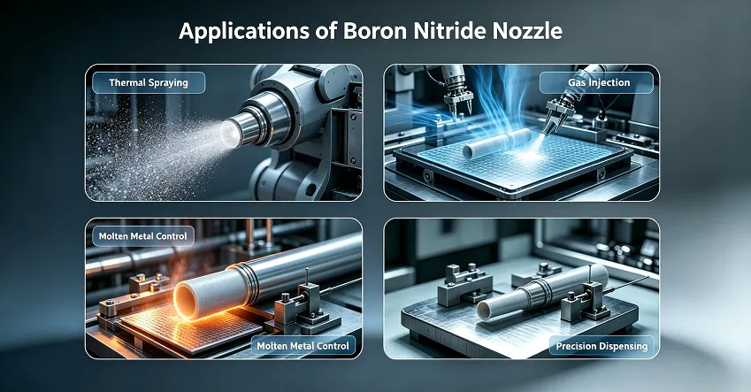
Compared with many extremely hard technical ceramics, machinable BN offers a significant manufacturing advantage. Selected BN grades can be machined into relatively complex shapes using appropriate tooling and processing conditions. This makes BN practical for customized semiconductor equipment components such as crucibles, rings, spacers, nozzles, shields, insulating supports, fixtures, and other precision structures. This characteristic is particularly useful during equipment development because semiconductor processes frequently require customized geometries rather than standardized ceramic shapes. Engineers may need thin walls, narrow grooves, holes, stepped structures, or complex internal profiles. BN’s machinability can reduce the manufacturing difficulty associated with such geometries.
Nevertheless, good machinability does not mean that BN can be processed without engineering controls. Cutting direction, tool geometry, machining speed, component thickness, edge design, and final surface condition can influence the integrity of the finished part. For precision applications, dimensional tolerances should therefore be specified together with flatness, concentricity, surface roughness, and edge requirements.

11. Company Profile: JianXun Technology Co., Ltd.
JianXun Technology Co., Ltd. focuses on advanced ceramic materials and engineered ceramic components for demanding industrial, high-temperature, electronic, and semiconductor-related applications. The company provides boron nitride solutions with attention to material purity, thermal conductivity, electrical insulation, dimensional accuracy, machining quality, and application-specific requirements.
For semiconductor applications, JianXun approaches BN component selection from an engineering perspective rather than relying on a single standard grade. Parameters such as operating temperature, process atmosphere, vacuum conditions, thermal conductivity, electrical resistivity, coefficient of thermal expansion, purity, density, surface roughness, dimensional tolerance, and thermal cycling can all be considered when determining the appropriate material specification.
For customized BN components, the engineering process can begin with the actual working conditions and component drawing. Based on the application, material grade, density, purity, thermal properties, machining requirements, and inspection criteria can then be established. This approach is particularly relevant to boron nitride semiconductor manufaturing, where process stability can depend on a combination of thermal behavior, contamination control, dimensional accuracy, and long-term material reliability rather than on a single material parameter.
12. FAQs about Boron Nitride
1. Why is Boron Nitride Suitable for Semiconductor Manufacturing?
Boron nitride is suitable for semiconductor manufacturing because it combines several properties that are difficult to obtain simultaneously from conventional engineering ceramics. High-purity hexagonal boron nitride provides excellent electrical insulation while offering relatively high thermal conductivity, low thermal expansion, good chemical stability, low density, and useful machinability. Depending on grade and orientation, BN ceramic components can provide thermal conductivity in the range of approximately 140–400 W/(m·K), electrical resistivity commonly exceeding 10¹³ Ω·cm, a density of approximately 1.8–2.2 g/cm³, and a low coefficient of thermal expansion that can be close to or below 4 × 10⁻⁶ K⁻¹ in relevant directions. This combination is particularly valuable in semiconductor equipment because components may need to dissipate heat without creating an electrical conduction path. In addition, BN can be machined into crucibles, rings, spacers, insulating supports, nozzles, fixtures, and other customized components, making it suitable for equipment where both material performance and dimensional accuracy are important.
2. What Properties of Boron Nitride Are Most Important for Semiconductor Processing?
For semiconductor processing, the most important BN properties normally include thermal conductivity, electrical resistivity, purity, thermal expansion coefficient, chemical stability, density, porosity, outgassing behavior, mechanical strength, and surface condition. Thermal conductivity determines how efficiently heat is distributed or removed from a process region, while electrical resistivity determines whether the component can provide reliable electrical isolation. High purity is important because metallic impurities or volatile contaminants can affect sensitive semiconductor processes. The coefficient of thermal expansion becomes particularly important when BN is assembled with silicon, quartz, graphite, alumina, aluminum nitride, or metallic components that have different thermal-expansion characteristics. Engineers should also consider the direction of heat flow because h-BN is anisotropic. A BN component with a nominal thermal conductivity of 200 W/(m·K) does not necessarily provide the same thermal performance in every direction. Therefore, boron nitride semiconductor manufaturing specifications should be established according to the complete process environment rather than selecting material based on one headline property.
3. How Does Boron Nitride Manage Heat While Maintaining Electrical Insulation?
The ability to conduct heat while remaining electrically insulating is one of the most important advantages of BN in semiconductor equipment. Hexagonal boron nitride has a layered crystal structure in which strong in-plane atomic bonding supports efficient phonon transport, while its wide electronic band gap prevents conventional electrical conduction. High-quality h-BN can exhibit in-plane thermal conductivity of several hundred W/(m·K), while its electrical resistivity can exceed 10¹³ Ω·cm depending on grade, temperature, purity, and measurement conditions. This combination allows a BN component to spread heat away from a localized hot zone without behaving like a metal electrically. In practical equipment design, this can be useful for electrically isolated thermal fixtures, high-temperature supports, process rings, insulating spacers, and thermal-management structures. However, engineers should evaluate thermal conductivity at the actual operating temperature and in the actual material orientation because phonon scattering, porosity, grain boundaries, and temperature can significantly change the effective thermal performance of the finished component.
4. Why Is the Anisotropy of Hexagonal Boron Nitride Important in Semiconductor Components?
The anisotropic nature of h-BN is directly related to its layered crystal structure and can have a significant influence on component performance. Thermal conductivity parallel to the basal plane can be several times higher than conductivity perpendicular to the layers. Thermal expansion also differs between crystallographic directions. For example, representative literature values for the coefficient of thermal expansion of h-BN can range from approximately −1.5 to 3.8 × 10⁻⁶ K⁻¹ depending on orientation, temperature, and material form. This means that an engineer designing a BN heat-spreading component must understand the direction in which heat is expected to travel. If the primary heat path is parallel to the BN layers, a highly oriented material may provide substantially better thermal performance than an equivalent material with random grain orientation. Conversely, if heat must travel through the thickness, the lower cross-plane conductivity must be included in the thermal model. For precision semiconductor equipment, material orientation should therefore be treated as a design parameter rather than a secondary material characteristic.
5. How Does Boron Nitride Perform at High Temperatures?
Boron nitride has excellent high-temperature capability, particularly under vacuum and inert atmospheres. High-quality h-BN can remain stable at temperatures well above 1000 °C, and literature reports thermal stability approaching approximately 2800 °C in suitable inert environments for certain forms of BN. However, this value should not be interpreted as a universal operating temperature for every BN component. The actual maximum service temperature depends on atmosphere, oxygen concentration, material purity, density, porosity, surface condition, thermal gradient, mechanical loading, and exposure time. Oxidation becomes increasingly important in air or oxygen-containing environments, particularly at elevated temperatures. In semiconductor equipment, engineers should therefore specify conditions such as vacuum level, nitrogen or argon atmosphere, oxygen concentration, heating rate, holding temperature, and cycle frequency when evaluating BN. A component operating at 1800 °C in an inert environment may have completely different lifetime expectations from one exposed to an oxidizing atmosphere at the same nominal temperature.